Galvanic isolation from the network on two volumes. Galvanic isolation of the analog signal
Modern life is unthinkable without television. In many apartments you can find two, and sometimes three television receivers. Cable TV is especially popular. But what if you need to connect several TVs to one antenna cable? It is natural to use the "Chinese" double or even tee.
For example, like this one:
It was this double splitter that I installed on two TVs to receive cable TV channels. However, the reception quality left much to be desired, if the channels of the first meter range showed tolerably, then the channels of the second and UHF ranges were received with strong signal attenuation. Having disassembled the splitter, I found in it a small ferrite double ring and several turns of single-core wire:


The device is a high-frequency transformer with anti-phase winding windings. And in theory, it should exclude the mutual influence of the input circuits for receiving the RF signal, but in fact it only weakened it, apparently due to the fact that there was a galvanic connection
I decided to replace the transformer with ordinary ceramic capacitances (red flags) with a rating of several picofarads, thereby eliminating this galvanic connection:

There was no limit to my surprise, both TVs were shown as if only one was working, i.e. not the slightest hint of mutual influence and excellent reception on all bands.
Capacities fit in the splitter case:

The only thing I scold myself for is why this idea didn't occur to me earlier.
The series of articles consists of three parts:
Interference in the schemes.
During the normal operation of an electronic device, noise may appear in the circuit.
Interference can not only interfere with the normal operation of the device, but also lead to its complete failure.
Rice. 1. Interference in the useful signal.
You can see the interference on the screen of the oscilloscope by including it in the part of the circuit under study (Fig. 1). The duration of interference can be either very short (units of nanoseconds, the so-called "needles") or very long (several seconds). The shape and polarity of interference is also different.
The propagation (passage) of interference occurs not only through the wired connections of the circuit, but sometimes even between parts of the circuit that are not connected by wires. In addition, interference can be superimposed, summed up with each other. So, a single weak interference may not cause a failure in the device circuit, but the simultaneous accumulation of several weak random interferences leads to incorrect operation of the device. This fact complicates the search and elimination of interference many times over, since they take on an even more random character.
Sources of interference can be roughly divided into:
- External source of interference. A strong electromagnetic or electrostatic field near the device may cause malfunctions in the electronic device. For example, a lightning strike, high current relay switching, or electric welding work.
- Internal source of interference. For example, when turning on/off a reactive load (motor or electromagnet) in a device, the rest of the circuit may fail. An incorrect program algorithm can also be a source of internal interference.
To protect against external interference, the structure or its individual parts are placed in a metal or electromagnetic shield, and circuit solutions with less sensitivity to external interference are also used. From internal interference helps the use of filters, optimization of the algorithm of work, changing the construction of the entire circuit and the location of its parts relative to each other.
It is considered very elegant not to suppress all interference indiscriminately, but to deliberately direct them to those places in the circuit where they will die out without causing harm. In some cases, this way is much simpler, more compact and cheaper.
Estimating the probability of interference in circuits and ways to prevent them is not an easy task, requiring theoretical knowledge and practical experience. But nevertheless, with hardness, we can say that the probability of interference increases:
- with an increase in the switched current or voltage in the circuit,
- with increasing sensitivity of circuit parts,
- with an increase in the speed of the applied parts.
In order not to redo the finished design due to frequent failures, it is better to familiarize yourself with the possible sources and propagation paths of interference already at the design stage of the circuit. Since about half of all manifestations of interference are associated with "bad" power, it is best to start designing a device with a choice of how to power its parts.
Power supply interference.
Figure 2 shows a typical block diagram of an electronic device that consists of a power supply, a control circuit, a driver, and an actuator.
Most of the simplest robots from the series on this site are built according to this scheme.

Rice. 2. Joint power supply of the control and power parts.
In such schemes, two parts can be conditionally distinguished: control and power. The control part consumes relatively little current and contains any control or computing circuits. The power part consumes much more current and includes an amplifier and a termination load.
Let's consider each part of the scheme in more detail.
Rice. 2 a.
Source of power(Fig. 2 a.) may be "batteries" or a mains transformer power supply. The power supply may also include a voltage regulator and a small filter.
Rice. 2 b.
Control scheme- this is a part of the scheme (Fig. 2 b.), where any information is processed in accordance with the operation of the algorithm. Signals from external sources, for example, from any sensors, can also come here. The control circuit itself can be assembled using microcontrollers or other microcircuits, or on discrete elements.
Communication lines they simply connect the control circuit to the actuator driver, that is, they are just wiring or PCB tracks.
Rice. 2 in.
Executive device(Fig. 2 c.) is often a mechanism that converts an electrical signal into mechanical work, such as an electric motor or an electromagnet. That is, the actuator converts the electric current into another form of energy and usually consumes a relatively large current.
Rice. 2 y.
Since the signal from the control circuit is very weak, so driver or amplifier(Fig. 2d) is an integral part of many schemes. The driver can be executed, for example, on only one transistor or a special microcircuit, depending on the type of actuator.
As a rule, the main source of strong interference is the actuator. The interference that appeared here, having passed through the driver, spreads further along the power bus (Interference in Fig. 2 is shown schematically by an orange arrow). And since the control circuit is powered from the same power source, it is likely that this interference will also affect it. That is, for example, an interference that appears in the motor will pass through the driver and may lead to a failure in the control circuit.
In simple circuits, it is enough to put a high-capacity capacitor of about 1000 microfarads and a ceramic 0.1 microfarad in parallel with the power source. They will act as a simple filter. In circuits with consumption currents of about 1 ampere or more, to protect against strong interference of complex shape, you will have to install a bulky, complex filter, but this does not always help.
In many circuits, the easiest way to get rid of the effects of interference is to use separate power supplies for the control and power parts of the circuit, that is, the use of the so-called separate power supply.
Although separate power is used not only to combat interference.
Separate food.
On Fig. 3 shows a block diagram of a device. This circuit uses two power supplies. The power part of the circuit is powered by power supply 1, and the control scheme - from power supply 2. Both power sources are connected by one of the poles, this wire is common to the entire circuit and signals are transmitted relative to it over the communication line.

Rice. 3. Separate power supply for the control and power parts.
At first glance, such a circuit with two power supplies looks cumbersome and complicated. In fact, such separate power supply circuits are used, for example, in 95% of all household equipment. Separate power supplies there are just different windings of transformers with different voltages and currents. This is another advantage of separate power supply circuits: several units with different supply voltages can be used in one device. For example, use 5 volts for the controller, and 10-15 volts for the motor.
Looking at the diagram in Fig. 3, it can be seen that the interference from the power unit is not able to get into the control unit along the power line. Consequently, the need to suppress or filter it completely disappears.

Rice. 4. Separate power supply with a stabilizer.
In mobile structures, for example, mobile robots, due to the dimensions, it is not always convenient to use two battery packs. Therefore, a separate power supply can be built using a single battery pack. In this case, the control circuit will be powered from the main power source through a stabilizer with a low-power filter, Fig. 4. In this circuit, you need to take into account the voltage drop across the stabilizer of the selected type. Typically, a battery pack with a higher voltage than the voltage required by the control circuit is used. In this case, the operability of the circuit is maintained even with a partial discharge of the batteries.

Rice. 5. L293 with separate power supply.
Many driver microcircuits are immediately specifically designed for use in separate power supply circuits. For example, the well-known L293 driver chip ( Rice. 5) has an output Vss- to power the control circuit (Logic Supply Voltage) and output Vs- to power the final stages of the power driver (Supply Voltage or Output Supply Voltage).
In all designs of robots with a microcontroller or a logic chip from the series, you can turn on the L293 with a separate power supply circuit. In this case, the supply voltage of the power part (voltage for motors) can be in the range from 4.5 to 36 volts, and the voltage can be applied to Vss the same as for powering a microcontroller or logic chip (usually 5 volts).
If the control part (microcontroller or logic chip) is powered through the stabilizer, and the power part is powered directly from the battery pack, this can significantly save energy losses. Since the stabilizer will only power the control circuit, and not the entire structure. This - another advantage of separate power supply: energy saving.
If you look again at the diagram of Figure 3, you can see that in addition to the common wire (GND), the power part with the control circuit is also connected by communication lines. In some cases, noise can also pass through these wires from the power section into the control circuit. In addition, these communication lines are often highly susceptible to electromagnetic influences ("pickup"). You can get rid of these harmful phenomena once and for all by applying the so-called galvanic isolation.
Although galvanic isolation is also used not only to combat interference.
Galvanic isolation.
At first glance, such a definition may seem incredible!
How can a signal be transmitted without electrical contact?
In fact, there are even two ways that allow this.
Rice. 6.
Optical signal transmission built on the phenomenon of photosensitivity of semiconductors. For this, a pair of an LED and a photosensitive device (phototransistor, photodiode) is used, Fig. 6.

Rice. 7.
A pair of LED-photodetectors are isolated in one housing opposite each other. This detail is called optocoupler(foreign name optocopler), Figure 7.
If a current is passed through the LED of the optocoupler, then the resistance of the built-in photodetector will change. This is how contactless signal transmission occurs, since the LED is completely isolated from the photodetector.
A separate optocoupler is required for each signal transmission line. The frequency of the optically transmitted signal can range from zero to several tens or hundreds of kilohertz.
Rice. eight.
Inductive signal transmission is based on the phenomenon of electromagnetic induction in a transformer. When the current in one of the windings of the transformer changes, the current in the other winding changes. Thus, the signal is transmitted from the first winding to the second (Fig. 8). This connection between the windings is also called transformer, and the transformer for galvanic isolation is sometimes referred to as isolating transformer.
![]()
Rice. 9.
Structurally, transformers are usually made on a ring ferrite core, and the windings contain several tens of turns of wire (Fig. 9). Despite the apparent complexity of such a transformer, it can be made independently in a few minutes. Ready-made small-sized transformers for galvanic isolation are also sold.
A separate such transformer is required for each signal transmission line. The frequency of the transmitted signal can range from several tens of hertz to hundreds of thousands of megahertz.
Depending on the type of transmitted signal and the requirements for the circuit, you can choose either transformer or optical galvanic isolation. In circuits with galvanic isolation on both sides, special converters are often installed to match (coupling, interfacing) with the rest of the circuit.
Consider now a block diagram using galvanic isolation between the control and power parts in Figure 10.

Rice. 10. Separate power supply and galvanic isolation of the communication channel.
According to this diagram, it can be seen that any interference from the power part has no way to penetrate the control part, since there is no electrical contact between the parts of the circuit.
The absence of electrical contact between parts of the circuit in the case of galvanic isolation allows you to safely control actuators with high-voltage power. For example, some kind of control panel powered by several volts can be galvanically separated from the mains phase voltage of several hundred volts, which increases safety for the operating personnel. This is an important advantage of circuits with galvanic isolation.
Control circuits with galvanic isolation can almost always be found in critical devices, as well as in switching power supplies. Especially where there is even the slightest chance of interference. But even in amateur devices, galvanic isolation is used. Since a slight complication of the circuit by galvanic isolation brings complete confidence in the smooth operation of the device.
Recently, circuits using powerful field-effect transistors have been increasingly used to switch loads in AC circuits. This class of devices is represented by two groups. The first category includes insulated gate bipolar transistors - IGBTs. The western abbreviation is IGBT.
The second, most numerous, includes traditional field (channel) transistors. This group also includes KP707 transistors (see Table 1), on which the load switch for the 220 volt network is assembled.
Primary AC is a very dangerous thing in every way. Therefore, there are many circuit solutions that allow you to avoid direct control of loads in the network. Previously, isolation transformers were used for these purposes, at present they have been replaced by a variety of optocouplers.
Transistor key with optical isolation
The scheme, which has already become typical, is shown in Figure 1. 
This circuit allows you to galvanically decouple the control circuits and the primary circuit of 220 volts. The optocoupler TLP521 is used as a decoupling element. You can apply other imported or domestic transistor optocouplers. The circuit is simple and works as follows. When the voltage at the input terminals is zero, the optocoupler LED is off, the optocoupler transistor is closed and does not shunt the gate of powerful switching transistors. Thus, on their gates there is an opening voltage equal to the stabilization voltage of the zener diode VD1. In this case, the transistors are open and work in turn, depending on the polarity of the voltage at a given time. Let's say there is a plus on the output pin of circuit 4, and a minus on terminal 3. Then the load current will flow from terminal 3 to terminal 5, through the load to terminal 6, then through the internal protective diode of the transistor VT2, through the open transistor VT1 to terminal 4. When the polarity of the supply voltage is reversed, the load current will flow through the diode of the transistor VT1 and the open transistor VT2. Circuit elements R3, R3, C1 and VD1 are nothing more than a transformerless power supply. The value of the resistor R1 corresponds to the input voltage of five volts and can be changed if necessary.
The whole circuit is made in the form of a functionally completed block. The circuit elements are mounted on a small U-shaped printed circuit board, shown in Figure 2. 
The board itself is attached with one screw to an aluminum plate with dimensions of 56x43x6 mm, which is the primary heat sink. Powerful transistors VT1 and VT2 are also attached to it through heat-conducting paste and mica insulating gaskets using screws with bushings. The corner holes are aligned both in the board and in the plate and serve, if necessary, for attaching the block to another more powerful heat sink.
Galvanic isolation. optocoupler circuit
| An optocoupler, also known as an optocoupler, is an electronic component that transmits electrical signals between two isolated electrical circuits using infrared light. As an insulator, an optocoupler can prevent high voltage from passing through the circuit. Transmission of signals through the light barrier occurs with the help of an IR LED and a photosensitive element, such as a phototransistor, is the basis of the optocoupler structure. Optocouplers are available in various models and internal configurations. One of the most common is an IR diode and a phototransistor together in a 4-pin package, shown in the figure.
Certain parameters must not be exceeded during operation. These maximum values are used in conjunction with the graphs to properly design the mode of operation.
On the input side, the infrared emitting diode has a certain maximum forward current and voltage, exceeding which will cause the emitting element to burn out. But even a signal that is too small will not be able to make it glow, and will not allow the impulse to be transmitted further along the circuit. Benefits of optocouplers
Disadvantages of optocouplers
Application of optocouplers
The versatility of optocouplers as elements of galvanic isolation and non-contact control, the variety and uniqueness of many other functions are the reason why the fields of application of optocoupler are computer technology, automation, communication and radio equipment, automated control systems, measuring equipment, control and regulation systems, medical electronics, visual display devices. Read more about the different types of optocouplers in this document. |


elwo.ru
Galvanic isolation: principles and scheme
Galvanic isolation is the principle of electrical isolation of the current circuit in question in relation to other circuits that are present in one device and improves technical performance. Galvanic isolation is used to solve the following tasks:
- Achievement of signal chain independence. It is used during the connection of various devices and devices, ensures the independence of the electrical signal circuit with respect to the currents that occur during the connection of different types of devices. Independent galvanic coupling solves the problems of electromagnetic compatibility, reduces the influence of interference, improves the signal-to-noise ratio in signal circuits, and increases the actual accuracy of measuring ongoing processes. Galvanic isolation with isolated input and output contributes to the compatibility of devices with various devices in difficult electromagnetic environments. Multichannel measuring instruments have group or channel isolation. The decoupling can be the same for several measurement channels or it can be channel-by-channel for each channel autonomously.
- Fulfillment of the requirements of the current GOST 52319-2005 on electrical safety. The standard regulates the resistance of insulation in electrical control and measurement equipment. Galvanic isolation is considered as one of a set of measures to ensure electrical safety, it must work in parallel with other protection methods (grounding, voltage and current limiting circuits, safety fittings, etc.).
Decoupling can be provided by various methods and technical means: galvanic baths, inductive transformers, digital isolators, electromechanical relays.
Solution diagrams for galvanic isolation
During the construction of complex systems for digital processing of incoming signals related to operation in industrial conditions, galvanic isolation must solve the following tasks:
- Protect computer circuits from critical currents and voltages. This is important if the operating conditions involve exposure to industrial electromagnetic waves, there are difficulties with grounding, etc. Such situations also occur in vehicles that have a large human influence factor. Errors can cause the complete failure of expensive equipment.
- Protect users from electric shock. The most common problem is relevant for medical devices.
- Minimize the harmful effects of various interference. An important factor in laboratories that perform accurate measurements, when building precision systems, at metrological stations.
Currently, transformer and optoelectronic isolations are widely used.
The principle of operation of the optocoupler
Optocoupler circuit
The light emitting diode is forward biased and only receives light from the phototransistor. According to this method, the galvanic connection of circuits is carried out, which are connected on one side with the LED and on the other side with the phototransistor. The advantages of optoelectronic devices include the ability to transmit communications over a wide range, the ability to transmit clean signals at high frequencies, and small linear dimensions.
Multipliers of electrical impulses
They provide the required level of electrical insulation, consist of transmitters-emitters, communication lines and receiving devices.
Pulse multipliers
The communication line must provide the required level of signal isolation; in the receiving devices, the pulses are amplified to the values necessary to start the thyristors.
The use of electrical transformers for decoupling increases the reliability of installed systems built on the basis of serial multicomplex channels in the event of failure of one of them.
Parameters of multiplex channels
Channel messages consist of information, command or response signals, one of the addresses is free and is used to perform system tasks. The use of transformers increases the reliability of the functioning of systems assembled on the basis of serial multicomplex channels and ensures the operation of the device in case of failure of several receivers. Due to the use of multi-stage transmission control at the signal level, high noise immunity indicators are provided. In the general mode of operation, sending messages to several consumers is allowed, which facilitates the initial initialization of the system.
The simplest electrical device is an electromagnetic relay. But galvanic isolation based on this device has a high inertia, relatively large dimensions, and can only provide a small number of consumers with a large amount of energy consumed. Such shortcomings prevent the wide application of relays.
Push-pull galvanic isolation can significantly reduce the amount of electrical energy used in full load mode, thereby improving the economic performance of the devices.
Push-pull decoupling
Due to the use of galvanic isolation, it is possible to create modern schemes for automatic control, diagnostics and control with high safety, reliability and stability of operation.
plast-product.ru
Galvanic isolation. Who, if not an optocoupler?
 There is such a thing in electronics as galvanic isolation. Its classical definition is the transfer of energy or signal between electrical circuits without electrical contact. If you are a beginner, then this wording will seem very general and even cryptic. If you have engineering experience or just remember physics well, then most likely you have already thought about transformers and optocouplers.
The article under the cut is devoted to various ways of galvanic isolation of digital signals. We will tell you why it is needed at all and how manufacturers implement an insulating barrier “inside” modern microcircuits.
Speech, as already mentioned, will focus on the isolation of digital signals. Further in the text, by galvanic isolation we mean the transmission of an information signal between two independent electrical circuits.
Why is it needed
There are three main tasks that are solved by decoupling a digital signal.
The first thing that comes to mind is high voltage protection. Indeed, providing galvanic isolation is a safety requirement for most electrical appliances. Let the microcontroller, which naturally has a low supply voltage, set the control signals for a power transistor or other high voltage device. This is more than a common task. If there is no isolation between the driver, which increases the control signal in terms of power and voltage, and the control device, then the microcontroller runs the risk of simply burning out. In addition, input-output devices are usually associated with control circuits, which means that a person who presses the “turn on” button can easily close the circuit and receive a shock of several hundred volts. So, galvanic isolation of the signal serves to protect people and equipment.  No less popular is the use of microcircuits with an insulating barrier to interface electrical circuits with different supply voltages. Everything is simple here: there is no “electrical connection” between the circuits, so the signal, the logical levels of the information signal at the input and output of the microcircuit, will correspond to the power supply at the “input” and “output” circuits, respectively.
  Galvanic isolation is also used to increase the noise immunity of systems. One of the main sources of interference in radio-electronic equipment is the so-called common wire, often the body of the device. When transmitting information without galvanic isolation, the common wire provides the total potential of the transmitter and receiver necessary for transmitting the information signal. Since the common wire usually serves as one of the power poles, connecting various electronic devices to it, especially power ones, leads to short-term impulse noise. They are eliminated by replacing the "electrical connection" with a connection through an insulating barrier.
How it works
Traditionally, galvanic isolation is built on two elements - transformers and optocouplers. If you omit the details, then the former are used for analog signals, and the latter for digital. We consider only the second case, so it makes sense to remind the reader about who an optocoupler is. To transmit a signal without electrical contact, a pair of a light emitter (most often an LED) and a photodetector is used. The electrical signal at the input is converted into "light pulses", passes through the light-transmitting layer, is received by the photodetector, and is converted back into an electrical signal.

Optocoupler isolation has earned huge popularity and for several decades was the only technology for decoupling digital signals. However, with the development of the semiconductor industry, with the integration of everything and everything, microcircuits have appeared that implement an insulating barrier at the expense of other, more modern technologies. Digital isolators are microcircuits that provide one or more isolated channels, each of which "outperforms" an optocoupler in signal transmission speed and accuracy, in terms of noise immunity, and, most often, in cost per channel.
The isolation barrier of digital isolators is manufactured using various technologies. The well-known company Analog Devices uses a pulse transformer as a barrier in ADUM digital isolators. Inside the microcircuit housing there are two crystals and, made separately on a pollimide film, a pulse transformer. The crystal transmitter generates two short pulses along the front of the information signal, and one pulse along the decline of the information signal. The pulse transformer allows, with a slight delay, to receive pulses on the transmitter crystal, on which the inverse conversion is performed.

The described technology is successfully used in the implementation of galvanic isolation, in many respects superior to optocouplers, however, it has a number of disadvantages associated with the sensitivity of the transformer to interference and the risk of distortion when working with short input pulses.
A much higher level of resistance to interference is provided in microcircuits, where the isolation barrier is implemented on capacitances. The use of capacitors makes it possible to exclude direct current coupling between the receiver and transmitter, which in signal circuits is equivalent to galvanic isolation. 
If the last sentence excited you .. If you feel a burning desire to scream that there can be no galvanic isolation on capacitors, then I recommend visiting threads like this. When your rage subsides, please note that all of this controversy dates back to 2006. There, as in 2007, we, as you know, will not return. And insulators with a capacitive barrier have long been manufactured, used and work perfectly.
The advantages of capacitive decoupling are high energy efficiency, small dimensions and resistance to external magnetic fields. This allows you to create low-cost integrated insulators with high reliability. They are produced by two companies - Texas Instruments and Silicon Labs. These companies use different technologies for creating a channel, however, in both cases, silicon dioxide is used as a dielectric. This material has a high electrical strength and has been used in the manufacture of microcircuits for several decades. As a result, SiO2 is easily integrated into the crystal, and a dielectric layer a few micrometers thick is sufficient to provide an isolation voltage of several kilovolts. On one (for Texas Instruments) or both (for Silicon Labs) condenser pads are located. The crystals are connected through these pads, so the information signal passes from the receiver to the transmitter through the isolation barrier. Although Texas Instruments and Silicon Labs use very similar technologies for integrating the capacitive barrier onto the chip, they use completely different principles for transmitting the information signal.
Each isolated channel at Texas Instruments is a relatively complex circuit.

Consider its "lower half". The information signal is fed to RC chains, from which short pulses are taken along the rising and falling edges of the input signal, and the signal is restored using these pulses. This way of passing the capacitive barrier is not suitable for slow-changing (low-frequency) signals. The manufacturer solves this problem by duplicating channels - the "lower half" of the circuit is a high-frequency channel and is intended for signals from 100 Kbps. Signals below 100 kbps are processed in the "top half" of the circuit. The input signal is subjected to preliminary PWM modulation with a high clock frequency, the modulated signal is fed to the isolation barrier, the signal is restored by pulses from the RC chains and further demodulated. The decision-making circuit at the output of the isolated channel "decides" from which "half" the signal should be sent to the output of the microcircuit.
As you can see in the Texas Instruments isolator channel diagram, both the low and high frequency channels use differential signaling. Let me remind the reader of its essence.
Differential transmission is a simple and effective way to protect against common mode noise. The input signal on the transmitter side is “split” into two signals V+ and V- inverse to each other, which are equally affected by common-mode interference of different nature. The receiver subtracts the signals and as a result the noise Vsp is eliminated.

Differential transmission is also used in digital isolators from Silicon Labs. These microcircuits have a simpler and more reliable structure. To pass through the capacitive barrier, the input signal is subjected to high-frequency OOK (On-Off Keyring) modulation. In other words, "one" of the information signal is encoded by the presence of a high-frequency signal, and "zero" - by the absence of a high-frequency signal. The modulated signal passes without distortion through a pair of capacitances and is restored at the transmitter side.
In this article, we will focus primarily on the optical isolation of an analog signal. A budget option will be considered. Also, the main attention is paid to the speed of the circuit solution.
Methods for decoupling an analog signal
A small review. There are three main ways to galvanically isolate an analog signal: transformer, optical and capacitor. The first two have found the most use. Today there is a whole class of devices called isolation amplifiers or decoupling amplifiers (Isolated Amplifier). Such devices transmit a signal by means of its conversion (there is a signal modulator and demodulator in the circuit).
Fig.1. General scheme of isolation amplifiers.
There are devices both for transmitting an analog voltage signal (ADUM3190, ACPL-C87), and specialized devices for connecting directly to a current shunt (SI8920, ACPL-C79, AMC1200). In this article, we will not consider expensive devices, but we will list some of them: iso100, iso124, ad202..ad215, etc.
There is also another class of devices - decoupling optical amplifiers with linearizing feedback (Linear Optocoupler) these devices include il300, loc110, hcnr201. The principle of operation of these devices is easy to understand by looking at their typical connection diagram.

Fig.2. Typical circuit for decoupling optical amplifiers.
For more information on Isolation Amplifiers, you can read: A. J. Peyton, W. Walsh "Analog Electronics with Operational Amplifiers" (Chapter 2), also the AN614 "A Simple Alternative To Analog Isolation Amplifiers" document from silicon labs, there is a good comparison table. Both sources are available online.
Special microchips for optical signal isolation
Now to business! To begin with, let's compare three specialized microcircuits: il300, loc110, hcnr201. Connected according to the same scheme:

Fig.3. Test circuit for il300, hcnr201 and loc110.
The difference is only in the ratings for il300, hcnr201 R1, R3=30k, R2=100R, and for loc110 10k and 200R, respectively (I selected different ratings to achieve maximum performance, but at the same time not go beyond the permissible limits, for example, by the current of the emitting diode ). Below are waveforms that speak for themselves (hereinafter: blue is the input signal, yellow is the output signal).

Fig.4. Oscillogram of the transient il300.

Fig.5. Hcnr201 transient waveform.

Fig.6. Transient Waveformloc110.
Now consider the ACPL-C87B chip (input signal range 0..2V). To be honest with her, I fussed for a long time. I had two microcircuits available, after I got an unexpected result on the first, I handled the second very carefully, especially when soldering. I collected everything according to the scheme indicated in the documentation:

Fig.7. Typical scheme forACPL— C87 from the documentation.
The result is the same. I soldered ceramic capacitors directly near the power legs, changed the op-amp (of course I checked it on other circuits), reassembled the circuit, etc. What is actually the snag: the output signal has significant fluctuations.

Fig.8. Transient WaveformACPL— C87.
Despite the fact that the manufacturer promises an output signal noise level of 0.013 mVrms and for option "B" the accuracy is ±0.5%. What's the matter? Perhaps a mistake in the documentation, because it's hard to believe in 0.013 mVrms. Unclear. But let's look at the Test Conditions / Notes column opposite Vout Noise and at Fig. 12 of the documentation:

Fig.9. The dependence of the noise level on the magnitude of the input signal and the frequency of the output filter.
Here the picture becomes a little clearer. Apparently the manufacturer tells us that we can stifle these noises through the low-pass filter. Well, thanks for the advice (ironic). Why is it that all of this was turned out in such a cunning way. Most likely it is clear why. Below are graphs without and with output RC filter (R=1k, C=10nF (τ=10µS))

Fig.10. Transient WaveformACPL— C87 without and with output filter.
Use of general purpose optocouplers for signal decoupling
Now let's move on to the most interesting. Below are the diagrams I found on the internet.

Fig.11. A typical scheme for optical decoupling of an analog signal on two optocouplers.

Fig.12. A typical scheme for optical decoupling of an analog signal on two optocouplers.

Fig.13. A typical scheme for optical decoupling of an analog signal on two optocouplers.
This solution has both advantages and disadvantages. The advantage is a higher insulation voltage, the disadvantage is that two microcircuits can differ significantly in parameters, therefore, by the way, it is recommended to use microcircuits from the same batch.
I assembled this circuit on a 6n136 chip:

Fig.14. Decoupling transient waveform at 6N136.
It worked, but slowly. I tried to assemble on other microcircuits (such as sfh615), it turns out, but also slowly. I needed it faster. In addition, often the circuit does not work due to self-oscillations that occur (in such cases they say the ACS is unstable))) It helps to increase the value of the capacitor C2 fig. sixteen.
One friend advised a domestic optocoupler AOD130A. Face result:

Fig.15. Oscillogram of the transient decoupling on AOD130A.
And here is the diagram:

Fig.16: Decoupling diagram at AOD130A.
One potentiometer is needed (RV1 or RV2), depending on whether the output signal is less or greater than the input. In principle, it was possible to put only one RV=2k in series with R3=4.7k, or even leave only RV2=10k without R3. The principle is clear: to be able to adjust around 5k.
Signal transformer isolation chip
Let's move on to the transformer option. The ADUM3190 microcircuit is available in two versions at 200 and 400 kHz (I have ADUM3190TRQZ at 400), there is also a microcircuit for a higher isolation voltage ADUM4190. I note that the case is the smallest of all - QSOP16. Output voltage Eaout from 0.4 to 2.4V. In my microcircuit, the output bias voltage is about 100mV (seen in the oscillogram in Fig. 18). In general, it works well, but personally I'm not entirely satisfied with the output voltage range. Assembled according to the scheme from the documentation:

Fig.17. Diagram ADUM3190 from the documentation.
Some waveforms:

Fig.18. Oscillogram of the ADUM3190 transient.
Results
Summarize. In my opinion, the best option is the scheme for domestic ADO130A (where did they just get them?!). And finally, a small comparative table:
| Chip | tr+delay (according to oscillators), µs | tf+delay (according to oscillators), µs | Range voltage, V | Voltage insulation, V | Noise (oscill.) mVp-p. | Price** per piece, r (05.2018) |
|---|---|---|---|---|---|---|
| IL300 | 10 | 15 | 0-3* | 4400 | 20 | 150 |
| HCNR201 | 15 | 15 | 0-3* | 1414 | 25 | 150 |
| LOC110 | 4 | 6 | 0-3* | 3750 | 15 | 150 |
| ACPL-C87B | 15 | 15 | 0-2 | 1230 | nd | 500 |
| 6N136 | 10 | 8 | 0-3* | 2500 | 15 | 50 |
| AOD130A | 2 | 3 | 0.01-3* | 1500 | 10 | 90 |
| ADUM3190T | 2 | 2 | 0.4-2.4 | 2500 | 20 | 210 |
*- approximately (according to the assembled circuit with speed optimization)
** - the average price for the minimum.
Yaroslav Vlasov
P.S. AOD130A manufactured by Proton OJSC (engraved with their logo in a black case) is a good one. The old ones (the 90s in a brown case) are no good.
 Do-it-yourself stabilizer - diagrams and recommendations on how to make a rectifier
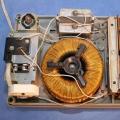 Voltage stabilizer circuit
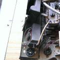 We extract radio components from various electronic trash How to make a radio receiver on a variable capacitor