Decoding POST codes. POST Codes AMI BIOS
Description: I bring to your attention the main Post-codes forBios. ManufacturerAMI.. Small accession. Immediately after pressing the POWER button on system block personal computer PC control goes directly to the BIOS. At this time (at the beginning of the PC start), the processor gives a signal on the BIOS chip, which initializes the boot-routine firmware load Base system I / O Program POST (Power-On Self Test) Tests the equipment installed on the computer, sets it up and prepares for work. For each individual equipment (processor, memory, video card, keyboard, I / O ports, etc.), a separate test is performed. Each test has its own unique numbercalled a post code. POST code Recorded to the MANUFACTURING TEST PORT port (with 0080h) prior to the start of each individual POST procedure test. After the POST test code is recorded in the Manufacturing Test Port port, the procedure for testing the appropriate equipment begins. If the test procedure fails to fail the MANUFACTURING TEST PORT port, the POST code of the last procedure remains (which caused the error). If you find out the POST code of the last procedure, you can define a device that caused an error. POST-CODE reads can be done in several ways. Because BIOS is issued by several manufacturers, respectively, for each BIOS of a separate manufacturer has its own POST code table.
Boot-Routine firmware calls the POST self-test subroutine.
This table contains post-codes that are displayed with the full POST procedure.
- CF is defined by the processor type and read / write CMOS
- C0 is pre-initialized by the chipset and L1-, L2-cache, programmed interrupt controller, DMA, timer
- C1 detected type and volume random access memory
- C3 BIOS code is unpackled in a temporary area of \u200b\u200bRAM
- 0С Checks BIOS checksum
- C5 BIOS code is copied to shadow memory and control is transmitted to the Boot Block module
- 01 Xgroup module is unpackled by the physical address 1000: 0000H
- 02 Processor initialization. CR and MSR registers are installed
- 03 Determine I / O resources (Super I / O)
- 05 cleared screen and CMOS status flag
- 06 Checked coprocessor
- 07 The keyboard controller is determined and is tested.
- 08 The keyboard interface is determined.
- 09 Initialization of the Serial ATA controller
- OA is defined by the keyboard and mouse that are connected to PS / 2 ports.
- 0B Installed AC97 Sound Controller Resources
- OE Tests F000H memory segment
- 10 Defined type Flash memory
- 12 is tested by CMOS.
- 14 Set values \u200b\u200bfor chipset registers
- 16 Primary initializes the clock generator
- 18 Determined by the type of processor, its parameters and cache volumes L1 and L2
- 1B Initializes Interrupt Vector Table
- 1C Checks CMOS checksum and battery voltage
- 1D Defined Power Management Power Management System
- 1F Loading Matrix (for laptops)
- 21 Initializes Hardware Power Management System (for laptops)
- 23 The mathematical coprocessor, drive, the initialization of the chipset is tested
- 24 Updated processor microcode. Create a map of the distribution of resources of devices Plug and Play
- 25 PCI initial initialization: devices are listed, search for a VGA adapter, VGA BIOS recording at C000: 0
- 26 Sets the clock frequency on CMOS Setup. Synchronization of unused DIMM and PCI slots is disabled. The monitoring system is initialized (H / W Monitor)
- 27 The interrupt is allowed int 09h. The keyboard controller is initialized again.
- 29 MTRR registers are programmed, APIC is initialized. Programming the IDE controller. The frequency of the processor is measured. The video system BIOS extension is caused
- 2b search BIOS video adapter
- 2D Displays Award Screensaver, Information about the type of processor and its speed
- 33 Reset keyboard
- 35 Tests the first DMA channel
- 37 Testing the second channel DMA
- 39 Testing page registers DMA
- 3C adjusts the controller 8254 (timer)
- 3e Interrupt Controller Check 8259
- 43 The interrupt controller is checked
- 47 Tested ISA / EISA tires
- 49 The amount of RAM is calculated. Registers are configured aMD processor K5.
- 4E Programmable MTRR registers for SYRIX processors. Cash L2 and APIC are initialized
- 50 is defined USB bus
- 52 Testing RAM with display results. Cleaned extended memory
- 53 If CMOS cleaning is performed, the password for login is reset.
- 55 Displays the number of processors (for multiprocessor platforms)
- 57 Displays the EPA logo. Initial initialization of ISA PNP devices
- 59 Defines virus protection system
- 5B Tip output to run the BIOS update from a floppy disk
- 5D The Super I / O controller is launched and an integrated audio controller
- 60 Log in to CMOS Setup if the Delete key has been pressed
- 65 Initializes Mouse PS / 2
- 69 Includes Cache L2
- 6B Customize chipset registers according to BIOS Setup
- 6D Resources for ISA PNP and COM ports for integrated devices are assigned.
- 6F is initialized and the controller of flexible disks is configured.
- 75 IDE devices are detected and installed: hard drives, CD / DVD, LS-120, ZIP, etc.
- 76 Displays information about IDE devices
- 77 Initialized successive and parallel ports
- 7a is reset and preparing to work mathematical coprocessor
- 7C Defines the protection against unauthorized recording on hard drives
- 7f If you have errors, the message is displayed and the DELETE and F1 keys are expected.
- 82 Allocated memory for managing power and changes to the ESCD table.
- Screensaver is removed with the EPA logo. Password is requested if needed
- 83 All data are saved from a temporary stack in CMOS
- 84 Output to the display screen Initializing Plug and Play Cards
- 85 USB initialization ends
- 87 SYSID tables are created in DMI
- 89 Install the ACPI tables. Interrupts are assigned for PCI devices
- 8B Called BIOS additional ISA- or PCI controllers, with the exception of the video adapter
- 8D Install the parity control parameters for CMOS Setup. APM is initialized
- 8F IRQ 12 is allowed for "hot" mouse connecting PS / 2
- 94 Completion of the initialization of the chipset. Displays the distribution table of resources. Enable cache L2. Setting the transition mode for summer / winter time
- 95 Installs the frequency of the keyboard and state of the NUM LOCK
- 96 For multiprocessor systems, registers are configured (for CYRIX processors). The ESCD table is created. The DOS Time timer is installed according to the readings of the RTC CMOS clock. The sections of the boot devices are saved for use by built-in antivirus. The speaker notifies the end of the post. The MSIRQ FF table is created. BIOS INT 19H interrupt is performed. Log search in the first sector of the boot device
The abbreviated procedure is performed when installing the Quick Power On Self Test parameter in the BIOS.
- 65 Reset video adapter. The audio controller, input / output devices are initialized, the keyboard and mouse are tested. Checked the integrity BIOS.
- 66 Initializes cache memory. Created table of interrupt vectors. Initialized power management system
- 67 The CMOS checksum is checked and the power battery is tested. CMOS parameter chipsets
- 68 The video adapter is initialized
- 69 Adjusts the interrupt controller
- 6A Test RAM (accelerated)
- 6B Displays EPA logo, processor and memory test results
- 70 Displays a hint to enter the BIOS SETUP. Initialized mouse connected to PS / 2 or USB
- 71 Initializes Cash Controller
- 72 The chipset registers are configured. A list of Plug and Play devices is created. & Initializes Disc Controller
- 73 Initializes hard disk controller
- 74 initialized coprocessor
- 75 If necessary, the hard disk is protected from recording
- 77 If necessary, the password is requested and press F1 to Continue, Del to Enter Setup
- 78 Initialized Extension Boards with Own BIOS
- 79 Initialized Platform Resources
- 7a generated root RSDT table, DSDT, FADT devices tables, etc.
- 7D is going to information about the sections of the boot devices
- 7E BIOS is preparing to boot the operating system
- 7F The state of the NumLock indicator is set in accordance with the settings
- BIOS Setup.
- 80 invoked INT 19 and operating system starts
AMIBIOS8.0.
- D0 initialization of the processor and chipset. Check the checksum of the BIOS boot unit
- D1 Initialization of I / O ports. The keyboard controller is transmitted to the BAT self-test command
- D2 L1 / L2 cache prohibition. The volume of established RAM is determined
- D3 Configure memory regeneration schemes. It is allowed to use cache memory
- D4 Test 512 KB of memory. The stack is installed and the exchange protocol with cache
- D5 BIOS code is unpackled and copied to the shadow memory
- D6 Checks the BIOS checksum and keystrokes Ctrl + Home (BIOS Restore)
- D7 Control is transmitted to the interface module that unpacks the code to the Run-Time area
- D8 The code executed is unpackled from flash memory into operational. CPUID information is saved
- D9 Unpacked code is transferred from the area of \u200b\u200btemporary storage to segments 0E000H and 0F000H RAM
- DA restored CPUID registers. POST execution is transferred to RAM
- E1-E8, EC-EE Errors related to system memory configuration
- 03 Does NMI processing, parity errors, signals to the monitor. The area for the GPNV event log is reserved, the initial values \u200b\u200bof the variables from BIOS are installed.
- 04 The battery performance is checked and the CMOS checksum is calculated.
- 05 Initializes the interrupt controller and the vectors table is built.
- 06 Testing and prepares timer
- 08 The keyboard is tested (keyboard indicators are blinking)
- C0 Starting processor initialization. Do not use cache memory. APIC is defined
- C1 for multiprocessor systems is determined by the processor responsible for starting the system.
- C2 completes the assignment of the processor to start the system. Identification with CPUID
- C5 is determined by the number of processors, their parameters are configured.
- C6 Initializes Cache memory for faster passage POST
- C7 completes the initial initialization of the processor
- 0a The keyboard controller is determined.
- 0b Mouse search connected to port PS / 2
- 0C Checks Keyboard
- 0e are detected and initialized various input devices
- 13 initial initialization of chipset registers
- 24 Unpacked and initialized BIOS modules specific to the platform.
- The table of interrupt vectors is created and the processing of interrupts is initialized.
- 2A Using the DIM mechanism, devices are defined on local tires. Prepares for initialization video adapter, resource distribution table is built
- 2C Discovery and initialization of the video adapter, the video adapter is called BIOS
- 2E Search and Initialization additional devices I / O.
- 30 prepares for SMI processing
- 31 is initialized and activated ADM module
- 33 Initializes the simplified loading module
- 37 The AMI logo is displayed, the BIOS version, processor, the hint of the BIOS entry keys
- 38 With DIM, various devices on local tires are initialized.
- 39 DMA controller is initialized
- 3A Sets the system time in accordance with the readings of the RTC clock
- 3B RAM is tested and results are displayed.
- 3C configure chipset registers
- 40 are initialized by successive and parallel ports, a mathematical coprocessor, etc.
- 52 According to the results of the memory test, the RAM data in CMOS is updated
- 60 BIOS SETUP Install the NumLock state is set and the auto signal parameters are configured.
- 75 The procedure is launched to work with disk devices (Interrupt INT 13H)
- 78 Creates a list of IPL devices (from which the operating system is possible)
- 7C Create and recorded in the NVRAM table of extended system configuration ESCD
- 84 Registration of errors found when executing POST
- 85 Displays messages about non-critical errors.
- 87 If necessary, BIOS SETUP is started, which is pre-unpackled in RAM
- 8C In accordance with the BIOS Setup, the chipset registers are configured
- 8D ACPI Tables are built
- 8E Customizable maintenance of non-promised interrupts (NMI)
- 90 is finally initialized by SMI
- A1 Cleaning the data that is not needed when loading the operating system
- A2 For interaction with the operating system, EFI modules are prepared
- A4 In Accordance With The Bios Setup Language Module Is Initialized
- A7 The final table of the POST procedure is displayed.
- A8 Sets the status of the MTRR registers
- A9 If necessary, waiting for command input from the keyboard
- AA removed POST interrupt vectors (INT 1CH and INT 09H)
- AB Definition devices for loading the operating system
- AC Following the steps of the chipset setting in accordance with the BIOS Setup
- B1 configures ACPI interface
- 00 Called Inte 19h Interrupt Processing (search for the boot sector, OS load)
Phoenixbios 4.0.
- 02 Verify Real Mode
- 03 DISABLE NON-MASKABLE INTERRUPT (NMI)
- 04 Get CPU Type
- 06 INITIALIZE SYSTEM HARDWARE
- 08 INITIALIZE CHIPSET WITH INITIAL POST VALUES
- 09 SET IN POST FLAG
- 0a Initialize CPU Registers
- 0b Enable CPU Cache
- 0C Initialize Caches to Initial Post Values
- 0E INITIALIZE I / O Component
- 0F Initialize The Local Bus IDE
- 10 Initialize Power Management
- 11 Load Alternate Registers with Initial Post Values
- 12 Restore CPU Control Word During Warm Boot
- 13 Initialize PCI Bus Mastering Devices
- 14 Initialize Keyboard Controller
- 16 (1-2-2-3) BIOS ROM Checksum
- 17 Initialize Cache Before Memory Autosize
- 18 8254 Timer Initialization
- 1A 8237 DMA Controller Initialization
- 1C RESET PROGRAMMABLE INTERRUPT CONTROLLER
- 20 (1-3-1-1) Test Dram Refresh
- 22 (1-3-1-3) Test 8742 Keyboard Controller
- 24 set es segment register to 4 GB
- 26 Enable A20 Line
- 28 AUTOSIZE DRAM
- 29 Initialize Post Memory Manager
- 2A Clear 512 KB Base Ram
- 2C (1-3-4-1) Ram Failure ON Address Line XXXX
- 2E (1-3-4-3) Ram Failure On Data Bits XXXX OF LOW Byte Of Memory Bus
- 2F Enable Cache Before System Bios Shadow
- 30 (1-4-1-1) RAM FAILURE ON DATA BITS XXXX OF HIGH BYTE OF MEMORY BUS
- 32 Test CPU Bus-Clock Frequency
- 33 INITIALIZE PHOENIX DISPATCH MANAGER
- 34 DISABLE POWER Button During Post
- 35 Re-Initialize Registers
- 36 Warm Start Shut Down
- 37 RE-INITIALIZE CHIPSET
- 38 Shadow System Bios Rom
- 39 RE-INITIALIZE CACHE
- 3A Autosize Cache.
- 3C Advanced Configuration of Chipset Registers
- 3D Load Alternate Registers With CMOS Values
- 40 CPU Speed \u200b\u200bDetection
- 42 Initialize Interrupt Vectors
- 45 POST Device Initialization
- 46 (2-1-2-3) Check Rom Copyright Notice
- 48 Check Video Configuration Against CMOS
- 49 INITIALIZE PCI Bus and Devices
- 4A Initialize All Video Adapters in System
- 4B QuietBoot Start (optional)
- 4C Shadow Video Bios Rom
- 4E Display Bios Copyright Notice
- 50 Display CPU Type and Speed
- 51 Initialize Eisa Board
- 52 Test Keyboard Keyboard Test
- 54 Set Key Click if Enabled
- 55 Initialize USB Bus
- 58 (2-2-3-1) Test for Unexpected Interrupts
- 59 Initialize Post Display Service
- 5A Display Prompt "Press F2 to Enter Setup"
- 5B Disable CPU Cache
- 5C Test Ram Between 512 and 640 KB
- 60 Test Extended Memory
- 62 Test Extended Memory Address Lines
- 64 Jump to Userpatch1
- 66 Configure Advanced Cache Registers
- 67 INITIALIZE MULTI PROSESSOR APIC
- 68 Enable EXTERNAL AND CPU CACHES
- 69 Setup System Management Mode (SMM) Area
- 6A DISPLAY EXTERNAL L2 CACHE SIZE
- 6B Load Custom Defaults (Optional)
- 6C Display Shadow-Area Message
- 6E Display Possible High Address for Umb Recovery
- 70 Display Error Messages are displayed error messages
- 72 Check for Configuration Errors
- 76 Check for Keyboard Errors
- 7C Set Up Hardware Interrupt Vectors
- 7D Initialize Hardware Monitoring
- 7E INITIALIZE COPROCESSOR IF PRESENT
- 80 DISABLE ONBOARD SUPER I / O PORTS AND IRQS
- 81 LATE POST Device Initialization
- 82 Detect and Install External RS232 Ports
- 83 Configure Non-McD IDE Controllers
- 84 Detect and Install External Parallel Ports
- 85 Initialize PC-Compatible PNP Isa Devices
- 86 RE-INITIALIZE Onboard I / O Ports
- 87 Configure MotheBoard Configurable Devices (optional)
- 88 INITIALIZE BIOS DATA AREA
- 89 Enable Non-Maskable Interrupts (NMIS)
- 8A Initialize Extended Bios Data Area
- 8B Test and Initialize PS / 2 Mouse
- 8C Initialize Floppy Controller
- 8F DETERMINE Number Of ATA Drives (Optional)
- 90 Initialize Hard-Disk Controllers
- 91 Initialize Local-Bus Harddisk Controllers
- 92 Jump to Userpatch2
- 93 BUILD MPTABLE FOR MULTI-PROSESSOR BOARDS
- 95 Install CD Rom for Boot
- 96 Clear Huge Es Segment Register
- 97 Fixup Multi Processor Table
- 98 (1-2) Search for Option Roms. One Long, Two Short Beeps On Checksum Failure
- 99 Check for Smart Drive (Optional)
- 9A Shadow Option Roms
- 9C Set Up Power Management
- 9D Initialize Security Engine (optional)
- 9E Enable Hardware Interrupts
- 9F Determine Number of ATA and SCSI DRIVES
- A0 Set Time Of Day
- A2 Check Key Lock
- A4 INITIALIZE TYPEMATIC RATE
- A8 Erase F2 Prompt
- AA Scan for F2 Key Stroke
- AC ENTER SETUP.
- AE CLEAR BOOT FLAG
- B0 Check for Errors
- B2 POST DONE - Prepare to Boot Operating System
- B4 (1) One Short Beep Before Boot
- B5 Terminate Quietboot (Optional)
- B6 Check Password (Optional)
- B9 Prepare Boot
- Ba Initialize Dmi Parameters
- BB INITIALIZE PNP OPTION ROMS
- BC CLEAR PARITY CHECKERS
- BD Display Multiboot Menu
- BE CLEAR SCREEN (Optional)
- BF Check Virus and Backup. Reminders.
- C0 TRY TO BOOT WITH INT 19
- C1 INITIALIZE POST ERROR MANAGER (PEM)
- C2 Initialize Error Logging
- C3 INITIALIZE ERROR DISPLAY FUNCTION
- C4 Initialize System Error Handler
- C5 PNPND DUAL CMOS (Optional)
- C6 INITIALIZE NOTEBOOK DOCKING (Optional)
- C7 INITIALIZE NOTEBOOK DOCKING LATE
- D2 unknown interrupt
- E0 Initialize The Chipset
- E1 Initialize The Bridge
- E2 Initialize The CPU
- E3 Initialize System Timer
- E4 INITIALIZE SYSTEM I / O
- E5 Check Force Recovery Boot
- E6 Checksum Bios Rom
- E7 Go to Bios
- E8 Set Huge Segment
- E9 Initialize Multi Processor
- EA INITIALIZE OEM SPECIAL CODE
- EB Initialize Pic and DMA
- EC INITIALIZE MEMORY TYPE
- ED Initialize Memory Size
- EE Shadow Boot Block
- EF System Memory Test
- F0 Initialize Interrupt Vectors
- F1 INITIALIZE REAL TIME CLOCK
- F2 Initialize Video.
- F3 INITIALIZE SYSTEM MANAGEMENT MODE
- F4 (1) OUTPUT ONE BEEP BEFORE BOOT
- F5 boot to mini dos
- F6 CLEAR HUGE SEGMENT
- F7 Boot to Full DOS
Original and reliable POST code tables can be found on the respective BIOS manufacturers: AMI and Award sites. Sometimes POST code tables are given in manuals to motherboards.
1. Test of software and accessible processor registers (post-codes: 01, 02).
2. Check the RAM regeneration period (POST code: 04).
3. Initialization of the keyboard controller (POST code: 05).
4. Preliminary validation of non-volatile memory (CMOS) and CMOS battery status (POST code: 07).
5. Initialization of the chipset set registers with defaults (POST code: BE, Hex).
6. Checking availability and definition of RAM (POST code: C1, Hex).
7. Determining the presence and size of external cache memory (POST code: C6, Hex).
8. Checking the first 64 KB of RAM (POST code: 08).
9. Initialization of interrupt vectors (POST code: 0a, Hex).
10. Checking the CMOS checksum (POST code: 0B, Hex).
11. Detection and initialization of the video controller (POST code: 0D, Hex).
12. Verification of the video memory (POST code: 0E, hex).
13. Checking the BIOS checksum (POST code: 0F, Hex).
14. Checking controllers and registers of DMA pages (Post-codes: 10,
11, Hex).
15. Checking the system timer (POST code: 14, Hex).
16. Check and initialization of interrupt controllers (Post-codes: 15 ... 18, Hex).
17. Initialization of expansion tire slots (Post-codes: 20 ... 2F, Hex).
18. Determining the size and verification of the main and extended memory (Post-codes: 30, 31, Hex).
19. Re-initialization of the chipset set registers in accordance with the values \u200b\u200bset in CMOS Setup (POST code: BF, HEX).
20. Initialization of the FDD controller (POST code: 41, Hex).
21. Initialization of the HDD controller (POST code: 42, Hex).
22. Initialization of COM and LPT ports (POST code: 43, Hex).
23. Detection and initialization of the mathematical coprocessor (POST code: 45, Hex).
24. Check the need to enter the password (POST code: 4F, \u200b\u200bHEX).
25. BIOS Expansion Initialization (POST code: 52, Hex).
26. Setting the Virus Protect, Boot Speed, Numlock, Boot Attempt in accordance with the values \u200b\u200bset in CMOS Setup (Post-codes: 60 ... 63, Hex).
27. Calling the procedure for loading the operating system (POST code: FF, HEX).
As can be seen from the above sequence, the ability to display diagnostic messages on the monitor screen appears only after initializing the video controller, and if the POST procedure stopped at one of the previous steps, then see what it is not possible.
POST-codes AWARD BIOS MEDALLION V 6.0
POST code (Hex) Check-made
Starting POST starting procedures from Flash BIOS
CF Early definition of the processor type. Recording results in CMOS. CMOS read / write functional test.
If the definition of a processor type or an entry in CMOS is over fails, the fatal error of the operation and the post is executed stops
C0 Preliminary initialization of the chipset.
Prohibition of the regions of the shadow RAM, turning off the cache L2. Cleaning cache L1.
Programming the following basic chipset registers.
- Interrupt controllers: reception at the front of IRQ, Master Controller - IRQ 00H \u003d int 8 ... IRQ 7 \u003d int 0FH, Slave Controller - IRQ 8 \u003d int 77h ... IRQ 15 \u003d int 77h.
- PPP controllers.
- Interval timer: Counter 0 - frequency division mode by 65,536 (18.2 Hz) to generate IRQ queries 0 system hours. Counter 1 - the generation of pulses for the DRAM regeneration (128 cycles is performed for 2 ms or the interval between the regeneration of two lines is about 15 μs). Counter 2 - Used to voicing the system speaker.
- RTC is initialized if the battery failure occurred. If the VCC failure (BAT) was not, then only registers responsible for the interaction of RTC and processor are initialized, but not hours
|
Check type, volume, senior address and ECC RAM. Check the first 256 KB RAM. |
|
|
Organization in this area of \u200b\u200btransit buffer, which from Flash BIOS |
|
|
copies BOOT BLOCK to check checksum |
|
|
Check the BIOS checksum and availability of BBSS label. If the checks are incorrect, |
|
|
the decision to partial damage to the Flash BIOS IC is made. If checks |
|
|
correct, then the buffer copies the unpacking program of the system BIOS |
|
|
Unpacking system BIOS in RAM, copying to the OSAM of the Optional System |
|
|
BIOS. BIOS Shading Preparation |
|
|
Copying the POST code performed in the E000H-F000H area of \u200b\u200bthe shadow RAM. |
|
|
Control the control of the BOOT BLOCK module. |
|
|
The beginning of the post from the shadow RAM. |
Check the integrity of the BIOS structure. If the control sums of the BIOS service checks are coincided, the execution of the RAM check continues, otherwise the control is transmitted to the BIOS recovery programs
POST implementation in the shadow RAM )
1 In the physical address 1000: 0000H, the BIOS module is unpaid - the XGroup program, which allows you to install all system board resources, including a system timer, interrupt controllers and PDPs, a mathematical coprocessor and default video controller
3 Performing early initialization of the Super I / O chip, the first stage was performed on the steps of the CFH and C0H algorithm
5 Installing the initial attributes of the video system.
Checking the CMOS status flag, its content is reset
7 Reset the input and output buffers of the keyboard controller (compatible with IC 8042 or 8742). The controller is part of the SUPER I / O chip
fees. Self-testing, initialization of the keyboard controller. Connection of the keyboard interface is allowed
|
Prohibition of interface connection computer mouse PS / 2. |
|
|
The type of keyboard interface is defined (PS / 2 or AT / DIN). Programmed |
|
|
keyboard controller. The use of the keyboard is allowed |
|
|
The PS / 2-mouse interface is still prohibited. |
|
|
For some systems - the definition of ports to which PS / 2-keyboard connected |
|
|
and mouse that can cause port reassignment |
|
|
Checking the shadow segment of F000H reading and writing cycles. This area |
|
|
will be used for DMI and ESCD. If the check is incorrect, then |
|
|
a beep and EFH error code is displayed in port 0080H |
|
|
If recorded and read data from the F000H segment do not coincide, |
|
|
the error and the execution of POST stops |
10 Definition of the type of Flash BIOS installed. Check allows you to select the corresponding recording program for the BIOS, with which the special Read Intelligent Identifier command is loaded. The command is also used by the procedures for modifying ESCD and DMI blocks, which can be overwritten both when booting and after it - when applying for applications to the functions of Plug and Play or DMI.
The BIOS code performed in the working session will be decoded and rewritten to the Run-Time Area area (F000H).
Programming chipset registers
12 Performing CMOS test chain. In the RTC clock, the power mode is installed. CMOS cells are used in the further storage of intermediate results during the initialization procedure. In particular, the default values \u200b\u200bare loaded into the cells.
14 Performing early initialization of the chipset. At the first stage, resources inaccessible to the system board developer are programmed. At the second stage, the values \u200b\u200bchangeable using the Modbin utility are loaded into the chipset registers. It becomes possible to fine-tuning RAM and PCI devices
16 Early initialization of the system clock generator - setting default values
18 Defining processor parameters: manufacturer companies, family, generation, identification of the form and volume of cache L1 and L2, such as SMI. The execution of the function of the CPUID command (codes and architecture of processors of various manufacturers differ).
Check processor registers, measurement of the clock processor kernel. After performing the function, the result is placed in a 128-bit word formed by the cells of the central processor registers - EAX + EBX + ECX + EDX. To decrypt the value of the cache used, the code shifts and moves to the Al register
|
Initialization of interrupt vectors table (volume 1,024 byte, 256 types |
|
|
interrupts). At this stage, types for 32 vectors are installed (Int 00h- |
|
|
INT 1FH) indicating BIOS procedures. |
|
|
Checks aimed at providing Y2K requirements |
|
|
Checking the CMOS checksum and supply voltage matching |
|
|
battery Rate. If errors are detected - values \u200b\u200bare set |
|
|
defaults defined by the system board manufacturer |
|
At this stage, receiving scan codes from the keyboard and their processing controller 8742 and the processor are not possible, since interrupts are prohibited, the BIOS data area is not prepared, and the keyboard is not initialized. Setup BIOS settings should not contradict the execution of the POST sequence
21 Initialization of the Hardware Power Management system for laptops.
Formation of a table of physical parameters, structures for maintenance of autonomous battery power, power saving functions when working hard drives, as well as operations for preserving the image of RAM on disk
23 Detection of mathematical coprocessor.
Check the number of cylinders - 40 or 80, as well as the type of installed floppy disk.
Performing early initialization of the chipset.
Preparation of a BIOS resource map designed to further install Plug and Play devices, as well as UVV on the PCI bus
24 In the Intel P6 and P7 generation processors, it is possible to organize access to the microprogram memory, which contains the execution algorithms for each machine command. At this stage, changes can be made to the microcode of firmware, allowing to upgrade algorithms or enter new microcodes intended for new machine commands. The microcode update procedure is performed as follows.
- Using the CPUID command, the processor is identified and its parameters are determined - Type (Type), family (Family), model (model) and frequency multiplication factor (stepping).
- From the module of the microcode update, stored in the BIOS, the desired block of 2,048 bytes is read and unpackled not in RAM, but in SM RAM.
- The microcode of the processor is updated.
For some Intel processors, additional identification is performed. Updated resource allocation card
Plug and Play devices are initialized. Resource information requested by Plug and Play devices is updated based on the scanning of data from CMOS, BIOS extensions located on the UVV expansion tires, as well as the information stored in the ESCD data block. Data entry in ESCD is postponed to the final stage of the post.
25 Early PCI Initialization. Enumeration of devices on the bus. Purpose of RAM and UVV resources.
Finding the video system device, BIOS extensions and record information to the C000: 0H area (segment address in the CS register: the address of the offset in the IP register)
26 Configuring the logic serving the Vendor Identification line.
Completion of the initialization of the system clock generator. Disable the synchronization of unused DIMM and PCI slots.
Initialization of the system of stresses and temperature monitoring system performed in accordance with the type of system board
At this stage, receiving scan codes from the keyboard and their processing controller 8742 and the processor are not possible, since interrupts are prohibited, the BIOS data area is not prepared, and the keyboard is not initialized. Setup BIOS settings should not contradict the execution of the POST sequence
27 Interrupt resolution int 09h. Re-initialization of the keyboard controller based on new data (interrupt vectors, chipset initialization).
For BIOS, a 16-character input buffer is formed and a memory area is installed for full functioning.
29 Programming the MTRR registers of the P6 generation processor, as well as the initialization of the APIC controller Pentium processors.
|
Programming chipset (for example, IDE controller) in accordance |
|
|
with installations in CMOS. |
|
|
Measurement of the internal frequency of the processor. |
|
|
Challenge BIOS Video Systems |
|
|
Initialization of the multilinguality module. |
|
|
Sending data to display on the display screen (Award Screensaver, type |
|
|
processor and its speed) |
|
|
Super I / O Chip Programming |
|
|
Checking the interrupt controller (compatible |
|
40 Checking Channel Masking 2 Interrupt Controller (compatible with IM 8259)
|
Verification of the functioning of the interrupt controller (compatible with IC 8259) |
|
|
Counting the shared memory by checking each double word each page 64 KB. |
|
|
Recording a program designed to verify the AMD family processors |
|
|
Programming the SYRIX MTRR processor registers. Initialization |
|
|
cache L2 generation P6 generation, as well as APIC initialization for P6 |
|
|
USB bus initialization |
|
|
Check all memory, cleaning extended memory |
55 For a multiprocessor platform, the number of processors is displayed.
57 Displays the Logo Screen Plug and Play. Early Initialization of Devices Plug and Play
59 Activating anti-virus protection resource - integrated antivirus Trend Anti-Virus
60 Stage that allows you to download the SETUP program.
Before this stage you must have time to press the corresponding key
65 PS / 2 Computer Mode Initialization
67 Preparation of information for the address space for the call function: INT 15H (the contents of the register AX \u003d E820H)
At this stage, receiving scan codes from the keyboard and their processing controller 8742 and the processor are not possible, since interrupts are prohibited, the BIOS data area is not prepared, and the keyboard is not initialized. Setup BIOS settings should not contradict the execution of the POST sequence
|
Enable cache L2. |
|
|
Programming the chipset registers in accordance with the elements described |
|
|
in SETUP and in the autoconfiguration table |
|
|
Assigning resources for all Plug and Play devices. |
|
|
Automatic distribution of COM ports for integrated devices |
|
|
in the event that the setup "auto" option is set |
|
|
Initialization of the floppy disk controller. |
|
|
Additional setting of floppy disk registers |
73 Optional Input Function Bios awdflash.exe update utility, if it is located on a floppy disk and a key combination is selected
75 Detection and installation of all IDE devices: hard drives, LS-120, ZIP, CD-R / RW, DVD, etc.
If an error is detected, the appropriate message is displayed, and the program awaits keystrokes.
If the error is not detected or pressed the key
Cleaning the screensaver with the EPA logo or manufacturer
82 Depending on the type of chipset and motherboard, the RAM is highlighted for power management.
The ESCD table includes the latest changes associated with power management.
After removing the screensaver with the EPA logo, the video mode is restored. Password request, if provided by CMOS installations
83 Data recovery from temporary storage stack in CMOS
84 Output to the message "Initializing Plugand Play Cards ..." about previously detected devices Plug and Play and parameters
85 USB initialization completion.
Defining the order of loading from SCSI hard drives
87 Switching the video system on text mode.
Construction of the SYSID table in the DNI area according to the System Management Bios specification.
For service network devices The UUID identifier is created (Universal Unique ID), as well as an identifier for download from devices Fire Wire IEEE 1394
At this stage, all major initialization procedures are completed. Preparation of the operating system is being prepared, the tables necessary for this table are compiled; arrays, structures are formed
89 If the SETUP program provides the use of the ACPI protocol, the corresponding tables are inserted into the top area of \u200b\u200bthe address space 4 GB
|
Scanning in PCI space BIOS extensions intended for |
|
|
implementing AOL (Alert ON LAN). Initialization of AOL. |
|
|
Allowing the use of logical support for non-disguised support |
|
|
interrupts NMI. |
|
|
Permission to use parity control of RAM modules |
|
|
For hot mouse connection PS / 2, IRQ 12 line is allowed. |
|
|
Service line IRQ 11, normalization of noise noise parameters of lines |
|
|
interrupt requests |
91 Preparation of conditions for servicing hard drives in Power Management mode. Operations of this type (Suspend to RAM) can be implemented in the operating system operating session.
Installing BIOS variables storing the basic addresses of consecutive and parallel ports that have BIOS expansion programs
93 Preparations for saving information about the sections of the boot devices
94 If SETUP is provided, the L2 cache is turned on. Programming the Boot Up Speed \u200b\u200bparameter.
Completion of the initialization of the chipset and power management system.
Removing the BIOS start screensaver, the resource allocation table is displayed on the monitor screen.
Setting up the processor registers of the AMD K6 family. The final update of the Intel P6 processor registers.
Ultimate Remote Pre Boot Remote Pre Boot Subsystem
95 Installing the automatic transition mode for winter / summer time Daylight Saving.
Programming the keyboard controller to the number of presses per second and waiting time before logging into the auto drive mode.
Reading the KBD ID keyboard identifier.
For the 101-button keyboard, the NumLock flag is set according to CMOS information
96 Saving information about the sections of boot devices.
In multiprocessor systems, the completion system setting is performed, the service tables and fields used in the operating system operating session are generated.
Configure CYRIX family processor registers.
Filling and adjusting the ESCD table according to the state of the Power Management system of the Plug and Play and ATAPI devices.
CMOS adjustment in accordance with the requirements of the Y2K protocol.
Installing the DOS Time system clock counter in accordance with the RTC CMOS readings. The time value from the format "Watch: Minutes: Seconds" is translated
in the clock (time intervals of pulses) of the interval timer of 18.2 Hz and recorded in the BIOS variable area - DOS Time.
At this stage, all major initialization procedures are completed. Preparation of the operating system is being prepared, the tables necessary for this table are compiled; arrays, structures are formed
Saving partitions of download devices for future use of Trend Anti-Virus anti-virus tools and Paragon Anti-Virus Protection.
Permission to use L1 cache.
On the system block speaker is generated by the end of the post. Building and saving the MSIRQ table.
Perform preparation for operating system boot
FF Transfer Management Boot Program-Download Program. Interrupting BIOS INT 19H.
The subroutine caused allows (in accordance with the option of the BIOS Features Set UP menu of the SETUP program) to poll the boot devices to search for the download sector. To download Information from sector Cylinder: 0, Head: 0, Sector:
1 Reads at 07C0: 0000H, after which the control of the FAR JMP command is transmitted to the beginning of this block.
Performing a program recorded in the boot sector
NOTE.
ECC.Error Correcting Code) - Error correction codeused in RAM modules, contributing increase fault tolerance PC. ECC allows you to correct the error in one discharge and detect in two discharges. Therefore, the computer, in the memory of which such codes are used, in the case of an error in one discharge can work without interrupt, and the data will not be distorted
BBSS.BOOT BLOCK SPECIFICATION SIGNATURE) - tagging signature Specification of the boot unit.
SMI(System Management Interrupt) - hardware, integrated into the processor, designed to manage power consumed. To maintain these components, a high priority interrupt is used.
Y2K.— requirements presented to commercial products of computer systems for provide functional compatibility, functionality and other parameters that occurred before and after 2000.
DMI(Desktop Management Interface) - protocol, allowing to ensure interaction software with components of system boards.
Mtrr.MEMORY TYPE RANGE REGISTSERS - registers of generation processors P6 and P7, in which data is entered, describing the properties of memory areas and determining the type of memory caffery.
APIC (ADVANCED PROGRAMMABLE INTERRUPTION CONTROLLER) - Improved programmable interrupt controller, included in the chipset. Processor generation P6 also it has a similar controller for multiprocessor use.
Msirq. (Microsoft IRQ Routing Map) - table cards distributions interrupts, standardized Microsoft.
SM RAM.(SYSTEM MANAGEMEN RAM) - one of the names of operational register memory a small container provided in the processor architecture, starting with Pentium Pro and above, designed to store service data.
In the case of inadequate completion of each of the processes, the algorithm moves on a special occasion, and POST BIOS MEDAllion generates codes noted below:
POST-codesspecialcases Award BIOS V 6.0 Medallion
System Event Code (System Events Codes)
Code activated when servicing APM or ACPI components (Power Management Debug Codes)
|
Energy saving with a power outage +12 in |
|
|
Go to operation mode with minimal power consumption |
|
|
Interrupt to exit energy saving mode |
|
|
Transition processor to power saving mode by reducing its clock |
|
|
Transition to partial energy saving mode using ACPI technology |
|
|
Using the SMI component for switching to power saving mode |
|
|
Processor transition to power saving mode using APM technology |
|
|
System transition to power saving mode using APM technology |
|
|
Translation of the system in full power saving mode |
|
Operational Fatal Error Message (System Error Codes)
|
ECC Code Processing Error |
|
|
Error hard disk When returning from the power saving mode |
|
|
Data discrepancy when writing to the F000H segment and read from it |
|
To reduce the passage time of the POST Award BIOS test program, you can use the Quick Power On Self Test option, which can be detected in the SETUP program. In this case, the modified version of the Award Software test is launched, which, unlike full version Programs are performed quickly.
POST AMI BIOS 8 V1.4 Codes
View of the display of test points
To display POST AMI BIOS checkpoints, POST Diagnostic Card diagnostic boards are used, indicators on system boards, as well as displays control aMI BIOS CHECKPOINT DISPLAY Points.
The display is a line of code in the lower right corner of the monitor screen, selectable during POST passage
The lack of using the display of control points codes is the impossibility of using this method with a disconnected video system.
Purpose of the initialization dispatcher device
In different periods of testing POST, the control is transmitted by a special about gram. dim devices initialization dispatcher (DEVICE INITIALIZATION MANAGER).
This program receives control from the BIOS if you need to check the SIS Dark or Local Piss Bus. There are several POST control points intended to run this program.
2AH Initialization of devices on the system bus.
38H initialization of IPL devices.
39H Indication of errors when initializing tires.
95H Initialization of tires controlled by BIOS extensions.
DEH - RAM configuration error.
DFH - RAM configuration error.
The messages generated by DIM are also displayed in the 80H diagnostic port and are stored in the information word in the process of checking.
The word in which the marked information is stored, contains a younger byte, which coincides with the system POST code. Senior byte is divided into two tetrades. Below is a description of the codes downloaded to the tetrad.
Fields of senior noterada.
Initialization of all devices on tires forbidden.
Initialization of static devices on tires for interest.
Initialization of information output devices on tires.
Initialization of information entry devices on tires.
Initialization of system boot devices (IPL) on tires for interest.
Initialization of devices general purpose On tires you are interested in.
Error message for tires for interest.
Initialization of devices managed by BIOS extensions (for all tires).
Initialization of BIOS bootable extensions corresponding to BIOS BOOT SPECIFICATION (for all tires).
Junior Tetrad.
System initialization procedures (DIM).
Bus connections for integrated system devices.
Tire Isa Plug and Play.
PCMCIA bus.
In the event that an RAM configuration error is detected, a cyclic sequence of DEH, DFH codes and configuration tests that can take the following values \u200b\u200bare found in the diagnostic port.
00 does not detected RAM.
01 Installed DIMM modules of various types.
02 Read from the SPD node (Serial Presence Detect) The DIMM module is failed.
03 The DIMM module cannot be used at this frequency.
04 The DIMM module cannot be used in this system.
05 Error in the younger memory page.
POST card or post tester is PCI fee Extensions having a digital indicator that displays the initialization codes Mat. payments. On this code can be found in which of the components of the board there is a malfunction. Codes are often dependent on the BIOS manufacturer. If there are no errors and the test is successful, then POST gives the code a non-changing value, for example on most mat.
The initialization completion is displayed code "FF". Also often, the Testers are installed the displayed voltages +5 +3.3 +12, -12.
To your attention, error codes suitable on the most BIOS:
| POST code | Description |
|---|---|
| D0 | Preliminary initialization of the chipset of the motherboard and processor. Check the BIOS checksum. The prohibition of the non-promised NMI interrupt. SUPER I / O controller checks, CMOS check. |
| D1 | The keyboard controller is performed by the process of self-testing (BAT-test). The initialization of I / O ports is performed. Initialization of the DMA controller. |
| D2. | Prohibiting the use of cache memory. The procedure for determining the amount of fixed memory is performed. |
| D3. | The formation of requests for the regeneration of dynamic RAM is checked. Permission to use cache memory. |
| D4. | Testing 512 KB in memory. The stack address is set, the cache memory is configured. |
| D5. | The system BIOS code is unpackled and overwritten in Shadow RAM (Shaded Memory). |
| D6. | The BIOS checksum is calculated and checking the CTRL + HOME key combination. If at least one of these conditions is performed, the BIOS recovery procedure is launched. |
| D7 | In the case of successful checksum checks, the BIOS control is transmitted to the InterfaceModule module, which performs unpacking the executable code in the Run-Time area. |
| D8. | Unpacking Run-Time-code from flash memory in RAM. CPUID information is stored in RAM. |
| D9 | The unpacked Run-Time code is transferred from the temporary storage area into RAM. Control is transmitted to the unpacked module. |
| DA | The CPUID registers are restored. POST procedure is performed. |
| E0 | Initialization of the floppy drive registers. The interrupt controller is initialized and setting the interrupt vectors. Enabling the first level cache. |
| E9. | Setting the floppy drive registers. |
| EA. | Checking read operation with ATAPI CD-ROM and disk memory. |
| EB. | Return to the control point E9 If errors occur during operations with ATAPI CD-ROM. |
| EF. | Return to the EB control point in case of errors when disk operations. |
| F0. | Search for recovery file with name amiboot.rom. |
| F1 | At the F1 point, the transition is performed if the recovery file is not found. |
| F5 | Disabling the first level cache. |
| FB. | Definition type Flashrom. Search in FlashRom partition for storing chipset settings. |
| F4. | A transition is performed to the F4 point if the recovery file with the name amiboot.rom has an incorrect size. |
| FC. | Zeroing the main Flash BIOS unit. |
| FD. | Programming the main Flash BIOS unit is performed. |
| FF. | The FF point is running in the event that Flash BIOS programming is successfully completed. Do not write from Flashrom. ATAPI equipment is shutdown. Regenerate CPUID value. |
| 03 | It is forbidden to process a non-promised interrupt (NMI), checking the parity errors. Initialization of the data area of \u200b\u200bthe current execution of the BIOS and the POST procedure is initialized. |
| 04 | Check the CMOS checksum and battery voltage. |
| 05 | Initialization of the interrupt controller and forming the table of interrupt vectors. |
| 06 | Preparation for the operation of the interval timer. |
| 08 | The keyboard controller is performed by the process of self-testing (BAT-test). Initialization of the CPU. |
| C0. | Prohibiting the use of cache memory. APIC controller initialization. Preparation of a processor to work. |
| C1. | Setting the parameters of the processor. |
| C2. | Identification of the processor using the CPUID command. |
| C5. | Determining the number of processors and setting their parameters. |
| C6. | Initialization of the processor cache. |
| C7. | Completion of the initial initialization process of the central processor. |
| 0a. | Initialization of the keyboard controller. |
| 0b. | A mouse is found connected using the PS / 2 interface. |
| 0c. | The keyboard search is performed. |
| 0E. | Search and initializing I / O devices. Interrupt capture INT 09H. Output to the BIOS logo screen. |
| 13 | The initial initialization of the chipset registers is performed. |
| 24 | Unpacking and initialization of the BIOS modules is performed. Preparation for initialization of interrupt vectors. |
| 25 | Completion of the initialization of the interrupt vectors. |
| 2a. | Devices are initialized on local tires (using the DIM-Device Initialization Manager mechanism). Preparation for the initialization of the video adapter. |
| 2s | Search and initialization of the video card. |
| 2e. | Search and initialization of additional I / O devices are performed. |
| 30 | SMI component initialization (System Management Interrupt) is initialized. |
| 31 | Unpacking the ADM module. Initialization and activation of ADM. |
| 33 | Initialization of the loader module. |
| 37 | Output to the monitor screen AMI logo, BIOS version information, information about the type of processor and its speed. Display on the key name monitor that can be used to enter the BIOS SETUP. |
| 38 | Devices are initialized on local tires (using the DIM-Device Initialization Manager mechanism). |
| 39 | The DMA controller is initialized. |
| 3A | Set system time in accordance with the readings of real-time clock (RTC). |
| 3b. | Testing RAM is performed with the subsequent display on the test results monitor. |
| 3c. | Setting the chipset registers. |
| 40 | The initialization of mathematical coprocessor, parallel and serial ports is performed. |
| 50 | Adjustment of memory management modules. |
| 52 | Information is adjusted to CMOS on the scope of RAM (according to the results of the RAM test). |
| 60 | Programming the keyboard controller to the auto repeat frequency and waiting time before entering the auto-repeat mode according to the BIOS Setup settings. Installing the NumLock indicator status according to the settings of the BIOS Setup. |
| 75 | Initialization of the INT 13H interrupt is performed, which is used to work with disk devices. |
| 78 | A list of devices are created from which the OS boot can be loaded. |
| 7A. | The initialization of the remaining BIOS extensions is performed. |
| 7c. | Creating and saving the ESCD table. |
| 84 | The compilation of error reports that were discovered during the POST procedure passes. |
| 85 | Conclusion to the error information monitor discovered during the POST procedure. |
| 87 | At this stage, it is possible to enter the BIOS SETUP program. |
| 8c. | Setting the chipset registers. |
| 8d. | The ACPI table is built. |
| 8e. | NMI interrupt service. Setting the peripheral parameters. |
| 90 | The final initialization of SMI is executed |
| A0. | Request a download password (if in bIOS settings SETUP is provided). |
| A1 | Clear data is performed that are not required to load the OS. |
| A2. | Preparation of EFI modules. |
| A4. | Language module is initialized. |
| A7. | Output to the monitor table of the final results of the POST procedure. |
| A8. | MTRR Register Programming (Memory Type Range Register). |
| A9. | Waiting for command input from the keyboard. |
| AA. | Reset Interrupts INT 1C, INT 09. Disable the procedure maintenance module (ADM). |
| AB | Definition of devices from which you can download the OS. |
| AC | The final stage of the initialization of the chipset registers in accordance with bIOS parameters Setup. |
| B1. | The ACPI interface is configured. |
| 00 | Interrupting BIOS INT 19H. Managing the download process is transmitted to the loader of the operating system. The OS load begins. |
Any computer repairer knows that POST Card PCI is used to diagnose malfunctions when repairing and upgrading IBM PC computers (or compatible with it).
Such cards in Russia and the CIS produces several companies: Master Kit (Moscow), E-Kit Post Cards, Ace Lab (N.Novgorod), BVG Group (Moscow), Epos: PCI Testcard (Ukraine), IC Book: IC80 (Ukraine ), Jelezo: Jpost Full (Ukraine), VL COMP: PC Analyzer (Belarus). There are foreign solutions, but we cannot find them in a free sale.
POST Card PCI is a computer extension board that can be installed in any free PCI slot (33 MHz) and is designed to display the POST codes generated by the BIOS OM computer, in a user-friendly form.
Conditionally, all post-cards can be divided into serial and extragrain (sets for self-assembly).
Overview of existing post-cards
Consider the shortcomings of post-cards of various manufacturers.
The PCI POST-cards in Russia in Russia is considered to be Ace Lab, which has a large OPSN in the production of software and hardware complexes for diagnostics and reionct of computers.
Master Kit POST CARD PCI NM9221 (self-assembly kit) / BM9221 (finished fee). One disadvantage - the seven indicator looks at the "muzzle down".
The advantages of this Post Card: Collected on the Plis of the EPM3XXX series that supports hot-socketing (more reliable, as it is less likely to burn POST Card) and operating at 3.3V (better compatibility with modern PCI2.3 and PCI3.0 specifications), support for new and Old chipsets due to replaceable firmware.
e-kit_02. Disadvantages of this Post Card: Collected on Plis Outdated EPM7xxx series that does not support hot-socketing (less reliable, as more likely to burn POST Card) and operating on 5.0V (there may be problems with modern PCI2.3 and PCI3.0).
Ace Lab PC-PST PCI-2. It is not convenient that the indicator looks down, but there is an opportunity to choose one of the 4 possible ports, from where information will be read.
Ace Lab PC Power PCI-2 - Full-featured software - hardware complex, which allows you to perform a number of diagnostic tests running from the ROM installed on the board oriented to identify system errors and equipment conflicts.
BVG GROUP DUAL POST. Advantages: A simple and cheap post-card. Made on the basis of FPGA Altera EPM3032ALC44-10. Five LEDs carrying on itself (power on PCI - -12V, + 12V, + 3.3V, + 5V, and RESET signal) and two seven-segment indicator on both sides of the board. The indicator can show one digit - this means that the PCI slot in which this test is inserted, the clock does not come.
A characteristic disadvantage of this card due to its trimming is the removal of clocking from the PCI slot, in which this card is installed after the POST step at which the generator is initialized (for Award BIOS - 26H), as a result of which postgrads are stopped displayed. The methods of "struggle" with this disease are as follows:
- If DETECT DIMM / PCI CLOCK is present in the BIOS Setup - the translation in Disable will not allow the generator to remove the frequency from unused slots, as a result of which the DUAL POST will work "as normal";), showing all "relying" postcodes.
- If the checked board has Sharing PCI SLOTS (typically, the long-distance processor two connector, who have one interrupt "for two"), then you can insert any "normal" PCI device in one of them (video, sound, network, etc. .), And in the other - the postcase. When initializing the generator, seeing the "full-fledged" PCI device on Sharing PCI Slots - often (depends on the specific BIOS card) does not remove the tact with both than successfully "will use" Dual POST.
BVG GROUP POST PRO. Instead of seven seventhers, an LCD display is used with a running string, but the cost of the map is about 300 USD, which is unreasonably high.
Epos: PCI Testcard. The advanced series "Master" from useful "beams" by and large allows you to additionally only select switches on the board diagnostic port in the 0-3FFH range, which is used to output post codes. Disadvantages of this Post Card: Collected on Plis Outdated EPM7xxx series that does not support hot-socketing (less reliable, as more likely to burn POST Card) and operating on 5.0V (there may be problems with modern PCI2.3 and PCI3.0). There is also information about the output of incorrect POST codes on some motherboards.
IC Book: IC80. The well-known representative of the "adults" postcases, a distinctive feature of which is the presence of not only "frills" in the field of monitoring, but also unique (not having analog) opportunities for debugging the system in step-by-step mode. The board has several distinctive features:
- Selection of addresses used for diagnostic purposes: 80H / 81H and 84H / 85H, 378H, 1080H
- The output of diagnostic codes is performed on two indicators.
- Display information on the external indicator
- Stand-BY voltage indication 3.3V
- Support for parity on the PCI bus
- PCI Server Tire Support
A small disadvantage: Step-by-step mode on new boards does not quite correctly work.
Jelezo: Jpost Full. It hangs on some motherboard (mostly Gigabyte) into the black screen after the first reboot.
VL COMP: PC Analyzer. A simple and cheap post-controller, the highlight of which is to combine in one constructive at once two types of postcases - for ISA and for PCI.
POST CARD PCI BM9222 with LCD Diplay
Today we will consider the PCI Post-card of the new generation Post Card PCI BM9222 production of the Moscow company Maskener Kit.
Specifications
- Power supply: +5 V.
- Current consumption, no more than: 100 mA.
- Tire frequency PCI: 33 MHz.
- Diagnostic port address: 0080H
- POST code indication: on the LCD in two rows of 16 characters (the first line - POST code in hexadecimal and via dash - the type of bios, the second line - the error description in the form of a running string).
- Tire PCI Signal Indication: LEDs on the front side of the board - RST (PCI Reset Signal) and
- CLK (PCI clock signal).
- PCI tire power supply voltage indicators: + 5V, + 12V, -12V, + 3.3V.
- Compatibility with chip sets: Intel, VIA, SIS.
- PCB size: 95.5 x 73.6 mm.
Design
Constructively POST Card PCI is made on a double-sided printed circuit board with a foil fiberglass with dimensions of 95.5 x 73.6 mm. In order to improve the electrical conductivity of the device's contacts, the slats are covered with nickel.
POST CARD PCI
Each time you turn on the computer that is compatible with the IBM PC, and before loading the operating system, the computer processor performs the BIOS procedure called "Self-On-Self-Test" - POWER (POWER ON SELF TEST). The same procedure is also performed when you click on the RESET button or when the computer is rebooting. To avoid misunderstandings, it should be noted here that in some special cases in order to reduce the time of the computer's download time, the POST procedure can be somewhat trimmed, for example, in Quick Boot mode or when you leave the Hibernate sleep mode.
The main purpose of the POST procedure is to check the basic functions and computer subsystems (such as memory, processor, motherboard, video controller, keyboard, flexible and hard disks etc.) before loading the operating system. This in some extent will insure the user from trying to work on a faulty system, which could lead, for example, to destroy user data on HDD. Before you start each of the tests, the POST procedure generates the so-called POST code, which is displayed at a specific address in the address of the computer input / output devices. If a malfunction is detected in the test device, the POST procedure simply "freezes", and the pre-output POST code uniquely determines how "hanging" occurred on the tests. Thus, the depth and accuracy of diagnostics using POST codes is fully determined by the depth and accuracy of the tests of the corresponding POST BIOS procedure "A computers.
It should be noted that the POST tables are different for various BIOS manufacturers and, due to the advent of new test devices and chipsets, are somewhat different even for different versions The same BIOS manufacturer. POST code tables can be found on the respective BIOS manufacturers: for AMI it http://www.ami.com, for Award - http://www.award.com, sometimes POST code tables are given in manuals to motherboards.
To display the POST codes in a user-friendly, a device called POST Card. The POST Card proposed for the PCI bus is a computer extension board inserted (when power off!) In any free PCI slot (33 MHz) and having a text indicator to display POST codes and text information About the current code. From the features of the work of this Post Card, I would like to note that after turning on the computer and before the first active RESET PCI signal appears on the POST Card indicator, the Greeting message "BM9222 Masterkit Postcard" is displayed.
In addition, the POST Card has LEDs reflecting the status of the CLK and RST Tires of the PCI bus.
Troubleshooting with POST Card PCI
The sequence of actions when repairing a computer using POST CARD looks like this:
1. Turn off the power of a defective computer.
2. Install POST Card in any free PCI Slot Motherboard.
3. Turn on the computer power.
4. If necessary, adjust the contrast (when installing LCD ScreenFor PLED - the adjustment is not required) image by pressing the buttons (long-distance from the motherboard, the button increases the contrast, the closest - reduces) or change the type of bios displayed - by pressing and holding one of the buttons and pressing the second (after pressing the buttons, change the type of bios displayed in the first line of the indicator after the error code). All of the above settings are saved when the power is turned off and are loaded at the next voltage supply to POST Card.
5. We read information on the POST Card indicator - this is a POST code on which the computer is "freezed", and its description in the second line.
6. Comprehensive probable reasons.
7. When power off, we make rearrangement of loops, memory modules and other components to eliminate malfunction.
8. Repeat items 3-7, seeking a sustainable passage of the POST procedure and start loading the operating system.
9. With the help of software utilities, we produce final testing of hardware components, and in the case of floating errors - we carry out a long run of the corresponding program tests.
When repairing a computer without using Post Card, paragraphs 3-6 of this sequence simply omit and from the side of the computer repair looks just like a fevering rearrangement of memory, processor, extension cards, power supply, and to top it all - the motherboard.
If large firms have a large stock of good components, then for small firms and individuals, the repair of a computer by installing obviously good components turns into a complex problem.
How is the computer with the use of POST-Card implemented in practice?
First of all, when you turn on the power, before starting work, the POST procedure should occur the RST (Reset) signal system, which is indicated on the Post Card changing the welcome message to other Post Card messages. If the shift does not occur within 2-4 seconds (the welcome display time is about 0.7 seconds) or one of the "No Codes" or "Reset" messages appeared on more than 1 second, then in this case it is recommended to turn off the computer immediately, pull out all the boards and Cables, as well as memory modules from the motherboard. In the system unit, you must leave the motherboard connected to the power unit with the installed processor and POST Card fee. If, with the subsequent enlarge of the computer, the system reset normally and the first post codes appear, then, obviously, the problem consists in temporarily extracted computer components; Perhaps also in incorrectly connected loops. By inserting memory consistently, the video adapter, and then other cards, and watching the POST codes on the indicator, detect a faulty module.
Let us return now to the case when the initial reset of the system does not even undergo (the Post Card indicator does not change the greeting message by other messages). In this case, a computer power supply unit is either defective, or the motherboard itself (defects the RESET signal generation chain) or the processor does not start. You can accurately accurately install a well-service power supply to the motherboard.
We now consider the case when the reset signal passes, but no post codes are displayed on the indicator (the message "No Codes" is held); At the same time, as previously described, a system consisting only from motherboard, processor, POST Card and power supply is tested. If the motherboard is completely new, then the reason can be enclosed in the incorrectly installed jumper of the motherboard. If all jumpers and processor are installed correctly, and the motherboard is still not started, the processor should be replaced with a well-complete processor. If it does not help, we can conclude a malfunction of the motherboard or its components (for example, the cause of the malfunction may be damaged information in Flash BIOS).
The main advantage of POST Card is that it does not require a monitor for its work. At the same time, the computer testing using POST Card is possible in the early stages of the POST procedure, when sound diagnostics are not available. Another important feature is the display of post codes on all types of bios that output codes at 0 × 0080), but not described in the ROM.
PLED indicator
This verification device is completed with the indicator with the displaying element of type PLED. The advantages of this type of display is that it has a high contrast and a wide viewing angle - it is very important because often the post fee has to be installed in the computer in the case when other boards are installed in adjacent slots (network, sound, etc.).
Multilingual support
POST-card allows you to display codes for various types of bios in various languages \u200b\u200b(English and Russian by default). BIOS type change is carried out by simultaneously pressing both buttons at once. This post card decrypts 3 types of bios in 2 languages \u200b\u200b(only 6 types). Russified BIOS in the title contains the "RU" string.
Rows themselves with the description of the codes are located with a chip 24C256 - 32KB Seeprom. This microcircuit is installed in the panel, and experienced users May remove it and reprogram another (newer or other language) version in case of its appearance on the website www.masterkit.ru. The update is regularly, with tracking the development trends of computer equipment.
If this code Not decrypt in your version, you should use the Internet to promptly search for the test type of the test, as well as write a letterwick letter in the company with an indication of this case, and in the subsequent version this code will be already enabled.
For reprogramming, you can use the NM9215 set (programmer) in conjunction with the adapter to this type of microcircuits NM9216 / 4.
Checking the RS System Block POST Card PCI Tester in practice
Computer component testing sequence:
1. Testing the processor.
2. Checking the checksum of the ROM BIOS.
3. Check and initialization of DMA controllers, IRQ and timer 8254.
After this stage, the audio diagnosis becomes available.
4. Checking memory regeneration operations.
5. Testing the first 64 KB of memory.
6. Loading interrupt vectors.
7. Initialization of the video controller.
After this stage, diagnostic messages are displayed.
8. Testing the full volume of RAM.
9. Testing keyboard.
10. Testing CMOS memory.
11. Initialization of COM and LPT ports.
12. Initialization and test of the FDD controller.
13. Initialization and test of the HDD controller.
14. Search for additional ROM BIOS modules and their initialization.
15. Calling the operating system bootloader (INT 19H, Bootstrap), if it is impossible to load the operating system, the Rom Basic start attempt (int 18h); If you fail to stop the system (HALT).
Passing tests
When passing each of the tests, the POST generates a post-code that is written to a special diagnostic register. The information contained in the diagnostic register becomes available for observation when installing the POST Card diagnostic board in the free slot and is displayed on a seventeenthycular indicator in the form of two hexadecimal digits. The diagnostic register address depends on the type of computer, in older versions it is: ISA, EISA-80H, ISA-COMPAQ- 84H, ISA-PS / 2- 90H, MCA-PS / 2-680H, 80H, some EISA- 300H.
First of all, it is necessary to determine the manufacturer of the BIOS motherboard. This can be done either on the sticker on the BIOS chip, or on the inscriptions that are displayed on the screen a similar serviceable motherboard. In Russia and the CIS, the most common BIOS firms ami and award are the most common. With the acquisition of some experience, in the first post, codes can be called the BIOS manufacturer with confidence.
POST code tables are different for various BIOS manufacturers and, in connection with the appearance of new tested devices and chipsets, differ even for various versions of the same BIOS manufacturer.
Historically, the POST code values \u200b\u200bin the respective tables of BIOS manufacturers are given as hexadecimal numbers in the range of 00H-FFH (0-55 in a decimal number system), so for ease of use of such tables, it is necessary to display POST codes in hexadecimal.
Fault codes
AWARD SOFTWARE INTERNATIONAL, INC.
Awardbios v4.51pg elite
A dynamically developing company Award Software in 1995 proposed a new decision in the field of low-level software AwardBIOS "Elite", more known as v4.50pg. The control point service mode has not changed in any widespread version V4.51, nor in the rare version v4.60. The suffixes P and G denote respectively support for the PNP mechanism and maintenance of energy saving functions (Green Function).
Performing POST starting procedures from ROM
C0. Ban external cache. BANK INTERNAL CACHE. Ban shadow ram. Programming DMA Controller, Interrupt Controller, Timer, RTC Block
C1.Determining the type of memory, the total volume and placement on the rows
C3.Check the first 256K DRAM for the organization of Temporary Area. Unpacking BIOS in Temporary Area
C5. POST code executed is transferred to Shadow
C6. Determination of presence, volume and type External Cache
C8. Checking the integrity of programs and tables BIOS
CF. Definition of processor type
POST ON POST in Shadow RAM
03 BANK NMI, PIE, AIE (ALARM INTERRUPT ENABLE), UIE (UPDATE INTERRUPT ENABLE). SQWV programmable frequency generation ban
04 Checking the formation of DRAM Regeneration Queries
05 Check and initialization of the keyboard controller
06 Memory Station Test, starting with the F000H address, where BIOS is located
07 Checking the functioning of CMOS and battery power
BE. Programming configuration registers of the southern and northern bridges
09 Initialization of the L2 Cache and the Cyrix processor caching registers
0a. Generation of interrupt vectors. Setting up Power Management Resources and Set SMI Vector
0b.Checking the CMOS checksum. Scanning tire PCI devices. Processor microcode update
0s Initialization of the keyboard controller
0d. Search and initialization of the video adapter. Setting up IoAPIC. Measurements of clock frequency, installation FSB
0E. MPC initialization. Test video memory. Dispute Award Logo
0F. Checking the first controller DMA 8237. Definition of the keyboard and its internal test. Checking the BIOS checksum
10 Checking the second controller DMA 8237
11 Check page registers of DMA controllers
14 Test channel 2 system timer
15 Test Register Masking Queries 1st Interrupt Controller
16 Test Register Masking Queries 2nd Interrupt Controller
19 Checking the passivity of the NMI unmasked interrupt request
30 Definition of Base Memory and Extended Memory. APIC setup. Program control mode Write Allocation
Preparation of tables, arrays and structures for the start of the operating system
31 The main memory test display on the screen. Initialization
32 Displays the screensaver Plug and Play Bios Extension. SUPER I / O Resource Setup. Programming Onboard Audio Device
39 I2C bus generator programming
3c. Installing the SETUP login software flag
3D PS / 2 Mouse Initialization
3E. Initialization of the External Cache Controller and Cache Permissions
Bf. Configuring chipset configuration registers
41 Initialization of the flexible disk subsystem
42 Disabling IRQ12 If PS / 2 MOUSE is missing. The hard disk controller software is performed. Scanning other IDE devices
43 Initialization of successive and parallel ports
45 Initialization of the FPU coprocessor
4E. Error Message Indication
4f. Password request
50 Restoration of the CMOS previously stored in RAM
51 The resolution of 32 bit access to HDD. ISA / PNP Resource Setup
52 Additional BIOS initialization. Setting the values \u200b\u200bof PIIX configuration registers. Formation of NMI and SMI
53 Installing DOS Time Counter in accordance with Real Time Clock
60 Installing Anti-virus protection Boot Sector
61 Finishing actions on the initialization of the chipset
62 Read keyboard identifier. Installing its parameters
63 Correction of ESCD, DMI blocks. Cleaning RAM
FF. Transmission of loading control. BIOS executes the int 19h command
Consider the procedure for testing the system block of a personal computer. We install the BM9222 tester in the free PCI motherboard slot. Turn on the power. BIOS - a computer boot program stored in the Motherboard ROM produces a serial survey of all the devices included in the system unit (processor, memory modules, hard drive, video card, controllers, optical drive, external periphery: mouse keyboard, etc.).
If all the peripheral devices of the system unit are working, then after the download is downloaded on the tester screen, the following inscription FFH will light up.
"We introduce a malfunction" in the system unit. Turn off the power and remove the memory module from the system unit.
After powering and downloading the computer, the 4EH RAM error code appears on the Tester screen.
The tester accurately determined that the memory in the system unit was "faulty". After turning off the power and return the memory module in its place, the tester showed the serviceability of a personal computer.
Similarly, you can define other peripheral error codes and quickly eliminate the malfunction, replacing the faulty block to the serviceable one.
conclusions
American Megatrends, Inc. (AMI)
The control points of the POST procedures performed in AMIBIOS were redesigned and supplemented in 1995 and so far have not undergone significant changes. The first description of POST codes or as AMI calls them - "Check Points" in their current form appeared in connection with the release of the nucleus V6.24, 15/07/95. Some changes are made to AMIBIOS V7.0, which is reflected in this document.
Features of performing starting procedures AMIBIOS
If 55H, AAH data appears during the starting port in the diagnostic port, do not match this information with POST codes - we are dealing with a typical test sequence, which includes the integrity of the data bus.
At the start stage, the output to the diagnostic port of the data is specific character for each platform. In some implementations, the first visualized code is associated with actions that AMI calls CHIPSET SPECIFIC STUFF. This procedure is accompanied by an output to port 80h CCH values \u200b\u200band performing a number of action to configure system logic registers. As a rule, CCH code occurs in those cases when system logic from Intel, built on the basis of the PIIX controller, is TX, LX, BX chipsets.
Some on-board I / O chips contain RTC and the clamp controller, which on the start are in the disconnected state. The goal of the BIOS is to separate these board resources for future use. In this case, the first starting procedure associated with the setting of the keyboard controller is accompanied by the 10H value output, then the RTC initialization is initialized, which indicates the appearance in the diagnostic port of the DDH code. It should be noted that the refusal of at least one of these resources will entail unarting of the motherboard as a whole at the first stage of the post.
On a number of boards, the initialization process begins with the translation of the CPU to the protected mode. In this case, after the first visualization code 43H, the post continues as described in the AMIBIOS documentation - the control is transmitted to the D0H point.
Unpaved initialization codes
Uncompressed Init Code Check Points
| Error code | Error description |
|---|---|
| EE | In modern implementations AMIBIOS, the first visualized code is associated with the declaration of the device with which the BIOS recovery is possible. |
| CC. | Initialization of CD system logic registers Type Flash ROM is not identified |
| CE | Discrepancy of checksums in the start BIOS CF Error access to the spare microcircuit Flash ROM |
| DD. | Early initialization of RTC, which is integrated into SiO chip |
| D0 | The prohibition of the non-promised NMI interrupt. Working out of the time delay to grow transient processes. Checking the Boot Block checksum, remains during the mismatch |
| D1 | Perform Memory Regeneration Procedure and Basic Assurance Test. Transition to 4 GB Memory Addressing Mode |
| D3. | Determination of volume and primary memory test |
| D4. | Return to the actual memory addressing mode. Early initialization chip set. Setting stack |
| D5. | Transfer POST Module from Flash ROM to transit area |
| D6. | If the checksum or Ctrl + Home is lost, the transition to the Flash ROM recovery procedure is performed (code E0) |
| D7 | Transfer of the management of the service program that performs the unpacking of the SIS-DARK BIOS |
| D8. | Full unpacking system BIOS |
| D9 | System BIOS Management Control in Shadow RAM |
| DA | Reading information from SPD (Serial Presence Detect) Dimm DB modules Setting up MTRR registers of the central processor |
| DC | The memory controller is programmed according to data obtained from SPD DE error of the system memory configuration. Fatal error |
| Df. | System memory configuration error. A beep 10 early |
| 11 | Return from STR status (Suspend to Ram) |
| 12 | SMRAM Access Restore (System Management RAM) |
| 13 | Repair memory regeneration |
| 14 | Search and initialization VGA BIOS |
Flash Rom Procedure Codes
BOOT BLOCK RECOVERY CODES
| Error code | Error description |
|---|---|
| E0 | Preparation for the interception of INT19 and the ability to start the system in simplified mode is checked |
| E1. | Installing interrupt vectors |
| E3. | Restoring CMOS content, BIOS search and initialization |
| E2. | Preparation of interrupt controllers and immediate memory access |
| E6. | Interrupt resolution from system timer and FDC |
| EC | Re-initialization of IRQ controllers and DMA ED drive initialization |
| EE | Reading the boot sector from the EF diskette disk operation error |
| F0. | File search AMIBOOT.ROM. |
| F1 | In the root directory, the amiboot.rom file is not found F2 reading FAT |
| F3. | Reading amiboot.rom. |
| F4. | The size of the amiboot.rom file does not match the volume of Flash ROM |
| F5 | Prohibition Internal Cache. |
| FB. | Definition of type Flash ROM |
| FC. | Erasing the main block Flash Rom |
| FD. | Programming Basic Flash Rom Block |
| FF. | Restart Bios. |
Unpacked System BIOS codes performed in Shadowram
Runtime Code IS Uncompressed in F000 Shadow Ram
| Error code | Error description |
|---|---|
| 03 | The prohibition of the non-promised NMI interrupt. Determination of the type of discharge |
| 05 | Stack initialization. Prohibition of memory caching and USB controller |
| 06 | Performing a service program in RAM |
| 07 | Processor Recognition and APIC Initialization |
| 08 | Checking checksum CMOS |
| 09 | End / Ins Standby Check |
| 0a. | Check battery failure |
| 0b. | Cleaning the keyboard controller buffer registers |
| 0c. | Keyboard Controller Transmit Test Team |
| 0E. | Search for additional devices serviced by keyboard controller |
| 0F. | Keyboard initialization |
| 10 | The keyboard is transmitted to the discharge command |
| 11 | If the End or Ins key is pressed, the CMOS 12 reset is executed. Transfer to the passive state of DMA controllers. |
| 13 | Initialization Chip Set and Cash L2 |
| 14 | Checking system timer |
| 19 | DRAM Regeneration Queries Test is performed |
| 1A. | Checking the duration of the regeneration cycle |
| 20 | Initialization of output devices |
| 23 | The keyboard controller input is read. Interviewed Keylock Switch and Manufacture Test Switch |
| 24 | Preparation for interrupt vectors |
| 25 | Interrupt vectors initialization completed |
| 26 | Through the key of the keyboard controller, the arch of the jumper TURBO SWITCH is interviewed |
| 27 | Primary USB controller initialization. Updating the starting processor microcode |
| 28 | Preparation for video mode |
| 29 | LCD initialization panel |
| 2a. | Search for devices serviced by additional ROM |
| 2b. | Initialization of VGA BIOS, checking its checksum |
| 2c. | Execution VGA BIOS. |
| 2d. | CONCLUSION INT 10H and INT 42H |
| 2e. | Search for CGA video adapters |
| 2f. | CGA adapter video memory test |
| 30 | Test CGA adapter scan |
| 31 | Error video memory or scan formation schemes. Search for an alternative video adapter CGA |
| 32 | Test video memory of an alternative CGA video adapter and scan patterns |
| 33 | Mono / Color Interview Status Poll |
| 34 | Setting text mode 80x25 |
| 37 | Video mode installed. Screen cleaned |
| 38 | Initialization of onboard devices |
| 39 | Display error messages in the previous step |
| 3A | Output "Hit Del" to enter CMOS Setup |
| 3b. | Beginning of preparation for memory test in protected mode |
| 40 | Preparation of GDT and IDT Descriptor Tables |
| 42 | Transition to protected mode |
| 43 | Processor in protected mode. Interrupts are allowed |
| 44 | Preparation for checking the line A20 |
| 45 | Test line A20. |
| 46 | RAM size definition |
| 47 | Test data recorded in Conventional Memory |
| 48 | Re-checking Conventional Memory |
| 49 | Test Extended Memory |
| 4b. | Memory reset |
| 4C. | Indication of the resetting process |
| 4d. | Record in CMOS Dimensions of Conventional and Extended Memory 4E Indication of the Real System Memory |
| 4f. | Advanced Test Conventional Memory |
| 50 | Conventional Memory Size Correction |
| 51 | Extended Extended Memory Test |
| 52 | CONVENTIONAL MEMORY and EXTENDED MEMORY SAVED |
| 53 | Treatment of postponed parity errors |
| 54 | Prohibition of the control of parity and processing of non-promised interrupts |
| 57 | Initialization of the memory region for Post Memory Manager |
| 58 | An invitation is displayed for entering CMOS Setup |
| 59 | Return processor in real mode |
| 60 | Check page registers DMA |
| 62 | Test register registers and long-length shipping controller DMA # 1 |
| 63 | Test register registers and the length of shipment of the DMA controller # 2 |
| 65 | Programming DMA controllers |
| 66 | Cleaning the Write Request and Mask Set Post registers |
| 67 | Programming Interrupt Controllers |
| 7f. | NMI request resolution from additional sources |
| 80 | Installed interrupt maintenance mode from the PS / 2 port |
| 81 | Keyboard interface test when reset errors |
| 82 | Setting the keyboard controller operation mode |
| 83 | Checking Keylock status |
| 84 | Verification of memory volume |
| 85 | Output to the screen of error messages |
| 86 | Setup System System Setup |
| 87 | Unpacking CMOS Setup program in Conventional Memory. |
| 88 | The SETUP program is completed by the user. |
| 89 | Completed status recovery after setup |
| 8b. | Memory Backup Additional BIOS Variables |
| 8c. | Programming configuration registers |
| 8d. | Primary initialization of HDD and FDD controllers |
| 8f. | Re-initialization of the FDD controller |
| 91 | Configuring hard drive controller |
| 95 | ROM SCAN is performed to search for additional BIOS |
| 96 | Additional system resource settings |
| 97 | Checking the signature and checksum of additional BIOS |
| 98 | Setting up System Management RAM |
| 99 | Installing timer counter and variable parallel ports 9A Formation of the list of serial ports |
| 9b. | Preparation of the area in memory for the test of the coprocessor |
| 9C. | Initialization of the coprocessor |
| 9d. | Information about the coprocessor is saved in CMOS RAM |
| 9e. | Identification of the type of keyboard |
| 9f. | Search for additional input devices |
| A0. | Formation of MTRR registers (Memory Type Range Registers) |
| A2. | Error messages at previous initialization stages |
| A3. | Setting the time characteristics of the keyboard auto drive |
| A4. | Defragmentation of unused regions RAM |
| A5. | Installing video mode |
| A6. | Screen cleaning |
| A7. | Transferring BIOS executable code Shadow RAM |
| A8. | Additional BIOS Initialization in the E000H segment |
| A9. | Return Management System BIOS AA USB Tire Initialization |
| AB | Preparation of the INT13 module for servicing disk services |
| AC | Building AIOPIC tables to support multiprocessor AD systems PREPARATION INT10 module for servicing video services |
| AE | DMI initialization |
| B0. | System Configuration Table B1 ACPI BIOS Initialization |
| 00 | INT19H Software Interrupt - Download Boot Sector |
FEATURES OF DEVICE INITIALIZATION MANAGER
In addition to the above POST code, the diagnostic port displays reporting on events during the execution process of Device Initialization Manager (DIM). There are several checkpoints that displays the initialization state of the system or local tires.
The information is displayed in the word format, the younger byte of which coincides with the system POST code, and the older byte indicates the type of initialization procedure. The older tetrade in the senior pate indicates the type of procedure performed, and the youngest determines the tire topology for its use.
Senior Tetrad
Junior Tetrad
If a system memory configuration error is detected, the port 80H is displayed in an infinite cycle DE code, DF code, configuration error code that can take the following values:
2. Award BIOS V4.51PG ELITE
Awardbios v4.51pg elite
A dynamically developing company Award Software in 1995 suggested a new decision in the field of low-level software - Awardbios "Elite", better known as v4.50pg. The control point service mode has not changed in any widespread version V4.51, nor in the rare version v4.60. The suffixes P and G denote respectively support for the PNP mechanism and maintenance of energy saving functions (Green Function).
POST ON POST in Shadow RAM
| Error code | Error description |
|---|---|
| 03 | BANK NMI, PIE, AIE (ALARM INTERRUPT ENABLE), UIE (UPDATE INTERRUPT ENABLE). SQWV programmable frequency generation ban |
| 04 | Checking the formation of DRAM Regeneration Queries |
| 05 | |
| 06 | The test area of \u200b\u200bmemory starting with the F000H address, where BIOS 07 is placed on checking the functioning of CMOS and battery power |
| BE. | Programming configuration registers of the southern and northern bridges |
| 09 | Initialization of L2 cache and Cyrix processor extended caching registers |
| 0a. | Generation of interrupt vectors. Setting up Power Management Resources and Set SMI Vector |
| 0b. | Checking the CMOS checksum. Scanning tire PCI devices. CPU microcode updating |
| 0s | Initialization of the keyboard controller |
| 0d. | Search and initialization of the video adapter. Setting up IoAPIC. Measurements of clock frequency, installation FSB |
| 0E. | MPC initialization. Test video memory. Dispute Award Logo |
| 0F. | Checking the first DMA 8237 controller. Definition of the keyboard and its internal test. Checking the BIOS checksum |
| 10 | Checking the second controller DMA 8237 |
| 11 | Check page registers of DMA controllers |
| 14 | Channel Test 2 System Timer 15 Test Register of Masking Queries 1st Interrupt Controller |
| 16 | Test Register Masking 2nd Interrupt Controller 19 Checking the passivity of the NMI non-disguised interrupt request |
| 30 | Definition of Base Memory and Extended Memory. APIC setup. Program control mode Write Allocation |
| Error code | Error description |
|---|---|
| 31 | The main memory test display on the screen. USB initialization |
| 32 | Displays the screensaver Plug and Play Bios Extension. SUPER I / O Resource Setup. Programming Onboard Audio Device |
| 39 | I2C bus generator programming |
| 3c. | Installing the SETUP login software flag |
| 3D | PS / 2 Mouse Initialization |
| 3E. | Initialization of the External Cache Controller and Cache BF Permissions Configuration Registers SETA CHIP |
| 41 | Initialization of the flexible disk subsystem |
| 42 | Disabling IRQ12 If PS / 2 MOUSE is missing. The hard disk controller software is performed. Scanning other IDE devices |
| 43 | |
| 45 | Initialization of the FPU coprocessor |
| 4E. | Error Message Indication |
| 4f. | Password request |
| 50 | Restoration of the CMOS previously stored in RAM |
| 51 | The resolution of 32 bit access to HDD. ISA / PNP Resource Setup |
| 52 | Additional BIOS initialization. Setting the values \u200b\u200bof PIIX configuration registers. Formation of NMI and SMI |
| 53 | |
| 60 | Installing Anti-virus protection Boot Sector |
| 61 | Finishing actions on initialization chip set |
| 62 | Read keyboard identifier. Installing its parameters |
| 63 | Correction of ESCD, DMI blocks. Cleaning RAM |
| FF. | Transmission of loading control. BIOS executes the int 19h command |
3. AWARD BIOS V6.0 Medallion
Awardbios v6.0 medallion.
The first mention of Award Medallion Bios, Version 6.0 dates back to May 12, 1999. The structure of the new product remained unchanged by saving the early (Early), late (LATE) and the final (System) phase of the hardware initialization phase. Effective changes affected the post algorithms, which was reflected in the new coding of control points, significantly expanding them to the scope of application. At the same time, in the new BIOS there was no place to be outdated technologies, such as EISA, and for this reason, the POST code has been abolished.
Performing POST starting procedures from ROM
At the early initialization stage, the BIOS software code is executed from the Boot Block (BOOT BLOCK) in Flash ROM, and is accompanied by an output to the diagnostic port of checkpoints 91h ... FFH
| Error code | Error description |
|---|---|
| 91 | Selecting the CF Platform Start Script Definition of the processor type |
| C0. | Ban external cache. BANK INTERNAL CACHE. Ban shadow ram. Programming the DMA controller, interrupt controller, timer, RTC C1 unit. Definition of the type of memory, total volume and placement on strings 0s checking checks |
| C3. | Check the first 256K DRAM for the organization of Temporary Area. Unpacking BIOS in Temporary Area |
| C5. | If the checksums coincided, the POST code executed is transferred to Shadow. Otherwise, the control is transmitted to the BIOS recovery procedure. |
| B0. | North Bridge initialization |
| A0-AF. | Hardware-dependent procedure for initializing system logic E0-EF Error in the process of initializing system logic |
Restoration BIOS.
POST ON POST in Shadow RAM
Late initialization is performed in RAM and continues until the custom menu is called - CMOS Setup. For this phase, POST is characterized by the use of the E000H memory segment, which employs the passage of control points from 01H to 7fh.
| Error code | Error description |
|---|---|
| 01 | Unpacking XGroup on the physical address 1000: 0000H |
| 03 | Early |
| 05 | Install the initial values \u200b\u200bof variables that specify the image attributes. CMOS status flag check |
| 07 | Check and initialization of the keyboard controller |
| 08 | Definition of the type of connected keyboard interface |
| 0a. | The procedure of the auto definition of the keyboard and mouse. The final settings of the keyboard controller using the PCI space registers |
| 0E. | F000H memory segment testing |
| 10 | Type definitions installed memory Flashrom. |
| 12 | Test CMOS. |
| 14 | Procedure for initializing chipset registers |
| 16 | Primary initialization of onboard frequency synthesizer |
| 18 | Definitions of the installed processor and the volume of its Cache L1 and L2 1B generation of the interrupt vectors |
| 1C. | |
| 1d. | Primary Setup Power Management System |
| 1f. | Loading from an external xgroup module keyboard matrix |
| 21 | Initialization of the Hardware Power Management subsystem |
| 23 | Testing the coprocessor. Definition type FDD drive. Preparatory stage to create PNP resource cards |
| 24 | Procedure for updating the microcode of the processor. Updating resource distribution card |
| 25 | Primary initialization and scanning Tire PCI |
| 26 | Configuring logic that serves VID (Voltage Identification Device). Initialization of the on-board stress monitoring system and temperatures |
| 27 | Re-initialization of the keyboard controller |
| 29 | APIC initialization included in the central processor. The frequency measurement on which the processor works. Configure system logic registers. Initialization of the IDE controller |
| 2a. | |
| 2b. | Search VGA BIOS. |
| 2d. | Output to the data processor data screen |
| 33 | RESET execution for a connected keyboard |
| 35 | Checking the first channel of the DMA 8237 controller |
| 37 | Checking the second channel of the DMA 8237 controller |
| 39 | Testing page registers DMA |
| 3c. | Adjust the Programmable Interval Timer controller (8254) |
| 3E. | Initialization Master Controller 8259 |
| 40 | Initialization Slave Controller 8259 |
| 43 | Preparation of the controller of interrupts to work. Interrupts are prohibited, their decisions are made later, after the memory test |
| 45 | Checking the passivity of the non-disguised interrupt request (NMI) |
| 47 | Execution of ISA / EISA tests |
| 49 | Determining the volume of basic and extended memory. Program control of WRITES ALLOTION mode by setting up AMD K5 registers |
| 4E. | Memory testing within the first megabyte and visualize results on the display screen. Initialization of caching schemes for single and multiprocessor systems, setting CYRIX M1 processor registers |
| 50 | USB initialization |
| 52 | Testing all available system memory, including a region for the built-in video controller (Shared Memory). Visualization of results on the display screen |
| 53 | Reset Password on Login |
| 55 | Visualization of the number of discovered processors |
| 57 | The initial initialization of ISA PNP devices, each of which is assigned to CSN (Card Select Number). Visualization of the EPA logo |
| 59 | Anti-virus support system initialization |
| 5b. | Start BIOS update procedures from the drive on flexible disks 5D initialization of SIO and AUDIO controllers |
| 60 | Access to CMOS Setup is open |
| 63 | PS / 2 Mouse Initialization |
| 65 | USB Mouse Initialization |
| 67 | Using IRQ12 PCI devices if in the PS / 2 Mouse system 69 Full Initialization of the L2 Cache Controller |
| 6b. | Initialization of the chipset according to CMOS Setup |
| 6d. | Setting up resources for ISA PNP devices in SiO 6F configuration mode Initialization of the flexible disk subsystem |
| 73 | Preliminary actions to initialize the rigid disk subsystem. On some platforms - Alt + F2 survey to launch AwardFlash |
| 75 | Search and initialization of IDE devices |
| 77 | Initialization of successive and parallel ports |
| 7A. | Software reset of the coprocessor, recording of the control word in the FPU CW 7C register Setting the protection against unauthorized recording on hard drives |
| 7f. | Display error messages. Del and F1 keys maintenance |
Preparation of tables, arrays and structures for the start of the operating system
Starting from the 82H code, POST configures the system according to CMOS settings. The final phase is performed from the Shadow RAM area (E800H segment) and completes the operating system management - FFH code.
| Error code | Error description |
|---|---|
| 82 | The area in the system memory for power management is highlighted. |
| 83 | Recovery of data from a temporary storage stack in CMOS |
| 84 | Displaying the message "Initializing Plug and Play Cards ..." |
| 85 | USB initialization is completed |
| 86 | Reserved, Cleaning Carry Flag |
| 87 | Building SYSID tables in DMI |
| 88 | Reserved, Cleaning Carry Flag |
| 89 | ACPI service table generation |
| 8A. | Reserved, Cleaning Carry Flag |
| 8b. | Search and initialization BIOS additional devices |
| 8c. | Reserved, Cleaning Carry Flag |
| 8d. | Parity Bit Certificate Container Service |
| 8e. | Reserved, Cleaning Carry Flag |
| 8f. | Permission of IRQ12 for "hot" connection manipulator "Mouse" 90 reserved, Cleaning Carry Flag |
| 91 | Platform Legacy-Resource Initialization |
| 92 | Reserved, Cleaning Carry Flag |
| 93 | Presumably not used |
| 94 | Final actions to initialize the main set of logic before loading the operating system. The initialization of the power management system is completed. The BIOS startup screen is removed, the resource allocation table is displayed. For processors of the AMD K6® family, specific settings are performed. Microc update for Intel Pentium® II family processors and above |
| 95 | Installing the automatic transition mode for winter / summer time. Programming the keyboard controller to the frequency of the auto drive |
| 96 | In multiprocessor systems, the final system settings are performed and service tables and fields are created. For CYRIX family processors, additional registers are completed. Building an ESCD table "Extended System Configuration Data". Installing the DOS Time counter according to Real Time Clock. The sections of boot devices are saved for the fatal use of built-in antivirus: Trend AntiVirus or Paragon Anti-Virus Protection. The system speaker is fed to the end of the post. MSIRQ table is built and saved |
A number of processes occurring in Award Medallion BIOS is denoted by special groups of control points. These include:
System Event Codes - control points of system events.
Power Management Debug Codes - checkpoints arising during the execution of APM or ACPI services.
SYSTEM ERROR CODES - Fatal error messages.
DEBUG CODES FOR MP SYSTEM - Points of initialization of multiprocessor platforms.
Features of accelerated passage Post
To reduce the system loading time, the user in CMOS Setup can select the Quick Power On Self Test option. In this case, the passage of POST will be accelerated by refusing to perform some procedures (Quick Boot).
The Quick Boot operation scheme replaces the late and final phase POST and does not affect the operation of the boot unit. Award Software offers the codification of the executable procedures of the accelerated passage of POST, different from the standard one. Quick Boot begins with an output to the diagnostic port of the control point of 65h and ends with a POST code 80h. The control is then transmitted to the operating system with the display of the usual FFH code for Award BIOS.
| Error code | Error description |
|---|---|
| 65 | Early initialization of the SiO controller, program reset video controller. Setting the keyboard controller, keyboard test and mouse manipulator. Initialization of the audio controller. Checking the integrity of BIOS structures. Unpacking Flash ROM service procedures. Freight Synthesizer Initialization |
| 66 | Initialization of L1 / L2 cache according to the results obtained by the CPUID command. Generating a table of vectors consisting of pointers to interrupt processing procedures. POWER MANAGMENT Hardware Initialization |
| 67 | Checking the accuracy of CMOS and battery nutrition. Setting the chipset registers according to CMOS settings. Initialization of the keyboard controller in the chipset. Formation of variables BIOS Data Area |
| 68 | Video system initialization |
| 69 | Setup I8259 Interrupt Controller |
| 6A | According to a special algorithm, an accelerated single-pass test of RAM |
| 6b. | Visualization of the number of discovered processors, the EPA logo and invitant output to start the AwardFlash utility. Configuring the resources of the built-in I / O controller in configuration mode |
| 70 | Invitations to enter Setup. PS / 2 initialization and USB Mouse |
| 71 | Cash controller initialization |
| 72 | Configuring system logic configuration registers. Forming a list of Plug and Play devices. Initialization FDD controller |
| 73 | HDD controller initialization |
| 74 | Initialization of the coprocessor |
| 75 | If the user is prescribed in the CMOS Setup installations, the Ide HDD recovery is performed. |
| 77 | Password request and message output: "Press F1 to Continue, Del to Enter Setup" |
| 78 | Initialization of the BIOS of additional devices on the ISA and PCI tires |
| 79 | LEGACY initialization platform resources |
| 7A. | Generate RSDT root table and DSDT, FADT devices tables, etc. |
| 7d. | Search for information about the sections of the boot devices |
| 7E. | Configuring BIOS Services and Services Before booting the operating system |
| 7f. | Installing the Numlock flag according to CMOS Setup |
| 80 | Transmission of operating system management |
POST implementation in power saving mode
One of the placform states when the contents of the RAM is saved on the hard disk, called Hibernate. In the ACPI specification ("Advanced Configuration and Power Interface Specification", Revision 2.0a from 31/03/2002) it is defined as S4 Energy Saving Mode (Non-Volatile Sleep). Return to full functioning involves a special way to pass POST.
The operation of the ACPI S4, as at the accelerated start, replaces the late and final phase POST. An essential point is to check in the boot block of the start script. Depending on which ACPI state is the system after the RESET hardware signal, the output solution is made from the S4 state, which begins with the output to the diagnostic port of the control point 90H and ends with a POST code 9fh.
| Error code | Error description |
|---|---|
| 90 | Early initialization of the SiO controller, program reset video controller. Setting the keyboard controller, keyboard test and mouse manipulator |
| 91 | Checking the accuracy of CMOS and battery nutrition |
| 92 | Initialization of system logic registers and onboard frequency synthesizer |
| 93 | CPUID Cache Memory Initialization |
| 94 | Generating a table of vectors consisting of pointers to interrupt processing procedures. POWER MANAGMENT Hardware Initialization |
| 95 | Scan PCI tires |
| 96 | Initialization of the built-in keyboard controller |
| 97 | Video system initialization |
| 98 | Displaying VGA adapter messages |
| 99 | Checking the first channel of the DMA8237 controller by recording and checking the registers of the base address and the length of the shipment block 9a Setting the I8259 interrupt controller |
| 9b. | PS / 2 initialization and USB MOUSE. Unpacking ACPI code. Cashcondroller initialization |
| 9C. | Configuring system logic configuration registers. Forming a list of Plug and Play devices. Initialization of FDD and HDD controllers |
| 9d. | The reservation of the PM region in the system memory is not performed if it is created in Shadow RAM or SMRAM. In some cases, repeated, completing the USB bus initialization, performed when the L1 cache is disconnected |
| 9e. | Setting up Power Management, which is part of the system logic. Initialization of SMI generation schemes and setting SMI vector. Programming resources responsible for monitoring system events PM |
| 9f. | Using the prohibition and resolution operation, the L1 / L2 cache memory is cleared and its current size is restored. The power saving mode management settings specified in CMOS Setup are saved in PM RAM. For mobile platforms Checking a return to full functioning after disconnecting all feed voltages (Zero Volt Suspend mode) |
4. PHOENIX BIOS 4.0 RELEASE 6.0
PHOENIX TECHNOLOGIES, Ltd.
One of the leaders in the development of low-level software Phoe-Nix Technologies timed to the windows95 output of the new version of Phoenixbios 4.0. The Intel Pentium processor family support is reflected in the name of intermediate revisions. One of the latter - Release 6.0 - the basis of all the available BIOS. With the advent of Release 6.1, there was no significant changes in the implementation of the POST procedures, and therefore it did not affect the indication of control points.
The distinctive feature of Phoenixbios is that if during the execution of POST, test errors 512 KB of the main memory (2ch, 2eh, 30h codes) appear, in port 80H is displayed additional Information In the word format, the bits of which identify the failed address line or the data cell. For example, the code "2c 0002" means that the memory failure is detected over the address line 1. The code "2E 1020" in this case will mean that a data lines fail to be detected 12 and 5 to the younger battery data tires. In 386SX systems, which uses a sixteen-bit data bus, the occurrence of an error during the execution stage of the code 30H is impossible
The output into the diagnostic port of the POST code is accompanied by an output on the system speaker of the audio signal. Sound signal formation scheme Next:
- Eight bit code is converted into four two bit groups
- The value of each group increases by one
- At the resulting value, a short beep is generated (for example: code 16H \u003d 00 01 01 10 \u003d 1-2-2-3)
Performing POST starting procedures from ROM
| Error code | Error description |
|---|---|
| 01 | Baseboard Management (BMC) Controller Initialization |
| 02 | Check the current processor mode |
| 03 | Prohibition of the implementation of non-promised interrupts |
| 04 | The type of installed processor is determined. |
| 06 | Initial installations of PIC and DMA registers |
| 07 | The area in memory intended for a copy of the BIOS is reset |
| 08 | Early initialization of system logic registers |
| 09 | Installing the POST Software Flag |
| 0a. | Initialization of processor software resources |
| 0b. | Permission of Internal Cache. |
| 0E. | SUPER I / O Resource Initialization |
| 0c. | Initialization of L1 / L2 Cache according to CMOS |
| 0F. | IDE initialization |
| 10 | Power Management Subsystem Initialization |
| 11 | Setting alternative register values |
| 12 | Installation of the MSW Register (Machine Status Word) |
| 13 | Early Initialization of PCI Devices |
| 14 | Initialization of the keyboard controller |
| 16 | Check Checkline ROM BIOS |
| 17 | Determination of Cache L1 / L2 |
| 18 | Initialization of the system timer 8254 |
| 1A. | Initialization of the DMA controller |
| 1C. | Reset the values \u200b\u200bof the programmable controller of interrupts |
| 20 | Checking the formation of DRAM regeneration requests |
| 22 | Checking the keyboard controller |
| 24 | Installing a selector for maintenance of a flat 4GB memory model |
| 26 | Resolution A20 line |
| 28 | Determination of the total memory |
| 29 | POST MEMORY MANAGER (PMM) Initialization |
| 2a. | Zeroing 640KB basic memory |
| 2c. | Testing address lines |
| 2e. | Failure for one of the data lines in the younger |
| 2f. | CHOICE OF THE MEMORY OF MEMORY CASH |
| 30 | Test available system memory |
| 32 | Definition of CPU clock parameters and tire frequency |
| Error code | Error description |
|---|---|
| 33 | PHOENIX DISPATCH MANAGER INITIALIZATION |
| 34 | Ban power off using ATX POWER Button |
| 35 | Settings for system logic registers that control the formation of time characteristics of memory access, I / O ports, system and local tires |
| 36 | Restart is performed with an unsuccessful transition to the next POST procedure. The procedure sequence manages Watch Dog Service |
| 37 | The process of configuring system logic registers is completed. |
| 38 | The contents of the Runtime module BIOS is unpackled and rewrites to the area intended for Shadow RAM |
| 39 | Re-initialization of the cache controller |
| 3A | Re-definition of the size of the cache L2 |
| 3b. | BIOS execution trace initialization |
| 3c. | Additional setting of logic registers to configure PCI-PCI bridges and support distributed PCI tires |
| 3D | System logic registers are configured in accordance with CMOS Setup |
| 3E. | Read Hardware Configuration. |
| 3E. | Rom Pilot Connection Check |
| 40 | Definition of CPU clock parameters |
| 41 | Rom Pilot Initialization - Remote Download Management |
| 42 | |
| 44 | Set Bios Interrupt |
| 45 | Initialization of devices until the PNP mechanism is turned on |
| 46 | According to a special algorithm, the BIOS checksum is calculated |
| 47 | I2O I / O Controllers Initialization |
| 48 | Search video adapter |
| 49 | PCI initialization |
| 4A. | Initialization of system video adapters |
| 4b. | Quiet boot is performed - a shortened system start sequence used to accelerated POST passage |
| 4C. | The contents of VGA BIOS rewrite to the transit region |
| 4E. | Visualization of the text string BIOS Copyright |
| 4f. | Memory Backup For boot device selection menu |
| 50 | Visuals processor type and its clock frequency |
| 51 | Initialization of the controller and EISA devices |
| 52 | Programming the keyboard controller |
| 54 | Activated key audio mode |
| 55 | |
| 58 | Search for non-listed interruption requests |
| 59 | POST DISPLAY SERVICE Procedure Initialization (PDS) 5A Output "Press F2 to Enter Setup" |
| 5b. | BANK CPU INTERNAL CACHE |
| 5C. | CONVENTIONAL MEMORY check |
| 5e. | Detect Base Address |
| 60 | Extended Memory check |
| 62 | Check Address Lines Extended Memory |
| 64 | Control of the control to the executable block generated by the system board manufacturer (PATCH1) |
| 66 | Setting the caching registers |
| 67 | Minimum APIC Controllers Initialization |
| 68 | L1 / L2 Cache Resolution |
| 69 | Preparing System Management Mode RAM |
| 6A | Visuals External Cache |
| 6b. | Setting CMOS Setup values \u200b\u200bby default |
| 6C. | Visualization of information by OB using shadow RAM |
| 6E. | Visualization of information about Upper Memory Blocks (UMB) |
| 70 | Output of error messages |
| 72 | Check the current system and information configuration in CMOS |
| 76 | Check keyboard error information |
| 7A. | Checking the status of software (System Password) or hardware (Key Lock Switch) keyboard lock |
| 7c. | Installing hardware interrupt vectors |
| 7d. | Power tracking system initialization |
| 7E. | Initialization of the coprocessor |
| 80 | It is prohibited to the onboard I / O controller SiO |
| 81 | Preparation for operating system boot |
| 82 | Search and definition of ports RS232 |
| 83 | Configuring external controllers IDE |
| 84 | Search and definition of parallel ports |
| 85 | ISA PNP Device Initialization |
| 86 | SIO controller onboard resources are configured in accordance with the CMOS Setup settings. |
| 87 | MCD Configuration (Motherboard Configurable Devices) |
| 88 | Installed values \u200b\u200bof block variables in the Bios Data Area area |
| 89 | The formation of a non-promised interrupt is allowed |
| 8A. | Setting the values \u200b\u200bof variables in the Extended Bios Data Area area |
| 8b. | PS / 2 Mouse Connection Circuit Check |
| 8c. | Initialization of the drive controller |
| 8f. | Defining the number of ATA devices connected |
| 90 | Initialization and configuration of hard drive controllers |
| 91 | Set the time parameters of hard drives in PIO mode |
| 92 | Control to the executable block generated by the system board manufacturer (PATCH2) |
| 93 | Building a multiprocessor configuration table |
| 95 | CD-ROM maintenance procedure selection |
| 96 | Return to Real Mode |
| 97 | Building MP Configuration Table |
| 98 | ROM SCAN procedure is performed |
| 99 | Checking the status of the SMART 9A parameter Content ROM corresponds to RAM |
| 9C. | Setting up Power Management Subsystem |
| 9d. | Initialization of resources to protect against unauthorized access |
| 9e. | Hardware interrupts are allowed |
| 9f. | Determined by the number of IDE and SCSI drives |
| A0. | Installing DOS TIME as RTC A1 Purpose of this code Unknown A2 Checking Status Key Lock |
| A4. | Setting the keyboard auto drive characteristics |
| A8. | Message "Press F2 to ENTER SETUP" is removed from the screen |
| AA. | The presence of the SCAN code of the F2 key is checked in the AC input buffer starts the SETUP program |
| AE | The restart flag performed by Ctrl + Alt + Del B0 is generated by the message "Press F1 to Resume, F2 to Setup" |
| B1. | POST B2 Flag is removed POST Procedure Completed |
| B4. | Issue a sound signal before loading |
| B5. | Quiet Boot phase completed |
| B6. | Password check if this mode is enabled in Setup B7 ACPI BIOS Initialization |
| B9. | Search for boot devices on USB bus BA initialization of DMI parameters |
| BB. | ROM SCAN Procedure Repeat |
| BC. | Reset trigger fixation of parity ram errors |
| BD. | The menu is visualized to select the boot device BE screen cleaning before loading the BF operating system Activation of anti-virus support |
| C0. | The INT 19H software interrupt processing procedure is launched - boot sector boot. The interrupt processing procedure is consistently attempting to load Boot Sector, polishing disk devices in the order prescribed setup |
| C1. | Initial initialization of the failure maintenance procedure (PEM) C2 Calling service procedures for error protocol |
| C3. | Visualization of error messages in the order of their arrival C4 Installation of initial state flags |
| C5. | Initialization of the Extended CMOS RAM Cell Block |
| C6. | Primary docking station initialization |
| C7 | Deferred docking station initialization |
| C8. | Performing BOOT BLOCK Test procedures for determining the integrity of BIOS structures |
| C9. | Check the integrity of external with respect to system BIOS structures and / or modules |
| CA. | Running Console Redirect to maintain remote keyboard CB emulation disk devices in RAM / ROM |
| CC. | Running Console Redirect to maintain video CD data exchanging support with PCMCIA |
| CE | Setting the light pen controller |
Fatal error messages
D10 error caused by an exception (Exception Error) D2 Calling the interrupt processing procedure from the non-identified source D4 error associated with the disorders of the issuance protocol and removing the D6 queries, output from the protected mode with the D7 Reset Software to save the status of the video adapter requires greater Memory amount than Available in SMRAM D8 Error in software forming a DA processor reset switching loss when returning to Real Mode DC Output from the protected mode with a reset software without a second initialization of the DD interrupt controller error when testing the extended memory DE keyboard controller error DF A20 Line Management Error 19
Performing procedures from Boot Block
| Error code | Error description |
|---|---|
| E0 | Setting the configuration registers of the chipset E1 initialization of the Northern and South Bridges |
| E2. | CPU initialization |
| E3. | Initialization of system timer |
| E4. | SUPER I / O Resource Initialization |
| E5 | Checking the recovery jumper status, whose installation is forcibly started BIOS Recovery Mode |
| E6. | Checking the BIOS checksum |
| E7. | Control is transmitted by BIOS if its checksum is calculated correctly E8 MPS Support Initialization |
| E9. | Transition to flat 4GB memory model |
| EA. | Initialization of non-standard equipment |
| EB. | Configure Interrupt Controller and Direct Memory Access |
| EC | By records and control readings using a special algorithm, a memory type is determined: FPM, EDO, SDRAM, in accordance with the result, Host Bridge configuration registers are configured |
| ED | By recordings and checks, the special algorithm is determined by the amount of memory banks and lines. In accordance with the result, Host Bridge configuration registers are configured (DRAM ROW BOUDARY) |
| EE | The contents of the BOOT BLOCK are copied to Shadow RAM EF Preparing SMM RAM for SMI handler |
| F0. | Memory test |
| F1 | Initialization of interrupt vectors |
| F2. | Real Time Clock Initialization |
| F3. | Initialization of the video subsystem |
| F4. | Audio generation before loading |
| F5 | Loading the operating system stored in Flash ROM |
| F6. | Return to Real Mode |
| F7. | Boot to Full DOS |
| F8. | USB controller initialization |
| FA ... FF. | PhDebug procedure interaction codes |
5. INSYDE BIOS MOBILE PRO
Insyde Software Corp.
Market insider mobile systems The firmly settled where loyalty to traditions and a conservative approach to building a BIOS is required. Having inherited source From SystemSoft, the company is constantly working on its improvement. The last of the revisions of MobilePro is actively used in Mitac and Clevo laptops, the documentation for which the ERROR CODES table is based on Insyde Software is called POST execution control points.
Control points of the boot unit
Despite the fact that the company Insyde Software has created its first BIOS in 1992, established model of the boot unit, "or Boot Loader, as the creators themselves called him," finally formed only by the end of 1995. From this point on, the starting procedure has received the numbering according to the creation date.
The most significant point from the point of view of the service engineer, which is the process of loading the computer system with InsyDeBIOS, becomes a device for displaying diagnostic codes. Although, as a rule, Boot Loader uses the standard MANUFACTURE "S Diagnostic Port 80H, in some cases, the output point output is performed only on Pio Port for Diagnostic Purpose), which is nothing but parallel port 378h. There are implementations in which the diagnostic codes sent to port 80h are duplicated to the parallel port.
| Error code | Error description |
|---|---|
| 00 | Starting point of the boot unit 01 Prohibition of the A20 line (not used) |
| 02 | CPU microcode update |
| 03 | Testing RAM |
| 04 | Transfer of the boot unit into RAM |
| 05 | Performing a boot unit from RAM |
| 06 | Forcing Flash Rom Recovery Procedure |
| 07 | Transfer of system BIOS to RAM |
| 08 | Verification of the system BIOS checksum |
| 09 | Running POST procedure |
| 0a. | Running Flash ROM Recovery Procedure With FDD Drive |
| 0b. | Frequency synthesizer initialization |
| 0c. | Completion of the BIOS recovery procedure |
| 0d. | Alternative Recovery Procedure Flash ROM with FDD |
| 0F. | Stop in case of fatal error |
| BB. | Early Initialization LPC SiO |
| CC. | Starting point of start recovery Flash ROM |
| 88 | Resolution of ACPI functions |
| 99 | Error when leaving the STR mode |
| 60 | Go to Big Real Mode mode |
| 61 | Initialization SM BUS. SPD data is saved in CMOS A0 Reading and analyzing SPD fields previously saved in CMOS A1 Initialization of the memory controller |
| A2. | Determination of logical DIMM module banks |
| A3. | Programming the DRB registers (DRAM ROW BOUDARY) |
| A4. | Programming DRA registers (DRAM ROW ATTRIBUTS) |
| AE | DIMM modules are found in the system, which are based on the Error Correcting Codes features (ECC) |
| AF | Primary initialization of memory controller registers displayed in memory space |
| E1. | The execution of the boot procedure stops if the DIMM module is not equipped with a SPD microcircuit |
| E2. | The type of DIMM module does not comply with the requirements of the system. |
| EA. | The minimum time between the activation of the DIMM lines of the module and the transition to the regeneration state does not comply with the system requirements. |
| EC | Register modules are not supported by ED Cas Latency modes |
| EE | The organization of the DIMM module is not supported by the motherboard |
Performing POST procedures from RAM
The most advanced insydebios solutions use a 16-bit display of test points. For this, ports 80H and 81H are used, the last of which is designed to expand standard diagnostics.
The study of control points is hampered by their irregular constructions, when the various processes are accompanied by the same codes in meaning. In dual diagnostic systems, there are generic helicities of other order: some post codes are displayed only in one of the ports without the usual duplication.
| Error code | Error description |
|---|---|
| 10 | Cash memory initialization check CMOS |
| 11 | Ban Lines A20. Installing controller registers 8259. |
| 12 | Definition of the boot method |
| 13 | Initialization of the memory controller |
| 14 | Search connected to the ISA video adapter bus |
| 15 | Setting system timer values |
| 16 | Installing system logic registers by CMOS |
| 17 | Counting total RAM |
| 18 | Testing Junior Page Conventional Memory |
| 19 | Checking the checksum image of Flash ROM |
| 1A. | Re-installation of interrupt controller registers |
| 1b. | Adapter video initialization |
| 1C. | Initialization of a subset of the adapter video registers compatible with the software model 6845 |
| 1d. | Initialization EGA adapter |
| 1e. | CGA adapter initialization |
| 1f. | Test page registers DMA controller |
| 20 | Checking the keyboard controller |
| 21 | Initialization of the keyboard controller |
| 22 | Comparison of the resulting amount of RAM with a value in CMOS |
| 23 | Autonomous Battery Power Check and Extended CMOS |
| 24 | Testing the DMA controller registers |
| 25 | Setting the DMA controller parameters |
| 26 | Formation of interrupt vectors |
| 27 | Accelerated Definition of Installed Memory |
| 28 | Protected mode |
| 29 | System Memory Test |
| 2a. | Output from protected mode |
| 2b. | Transferring SETUP procedures to RAM |
| 2c. | Running the video initialization procedure |
| 2d. | Re-search CGA adapter |
| 2e. | Re-search EGA / VGA adapter |
| 2f. | Displaying VGA BIOS messages screen |
| 30 | Custom procedure for initializing the keyboard controller |
| 31 | Checking the connected keyboard |
| 32 | Checking a query from the keyboard |
| 33 | Checking the keyboard status register |
| 34 | Test and reset system memory |
| 35 | Protected mode |
| 36 | Advanced memory test completed |
| 37 | Output from protected mode |
| 38 | Ban Lines A20. |
| 39 | Initialization of the Cash Controller 3A Checking the system timer |
| 3b. | Installing DOS Time Counter in accordance with Real Time Clock |
| 3c. | Initialization of the table of hardware interrupts |
| 3D | Search and initialization of manipulators and pointers |
| 3E. | Setting the status of the numlock key |
| 3F. | Initialization of successive and parallel ports |
| 40 | Configuring consecutive and parallel ports |
| 41 | Initialization FDD controller |
| 42 | Initialization HDD controller |
| 43 | Power Management Initialization for USB Tire |
| 44 | Search and initialization of additional BIOS |
| 45 | Re-setting the status of the Numlock key |
| 46 | Check the functionality of the coprocessor |
| 47 | PCMCIA initialization |
| 48 | Preparing for the start of the operating system |
| 49 | Control of control executable bootstrap code |
| 50 | ACPI initialization |
| 51 | Initialization Power Management |
| 52 | USB bus controller initialization |
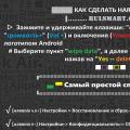 Firmware for HTC One SV from flash drive
 Why is the laptop heats and what to do about it?
 Reset to factory SAMSUNG smartphones